

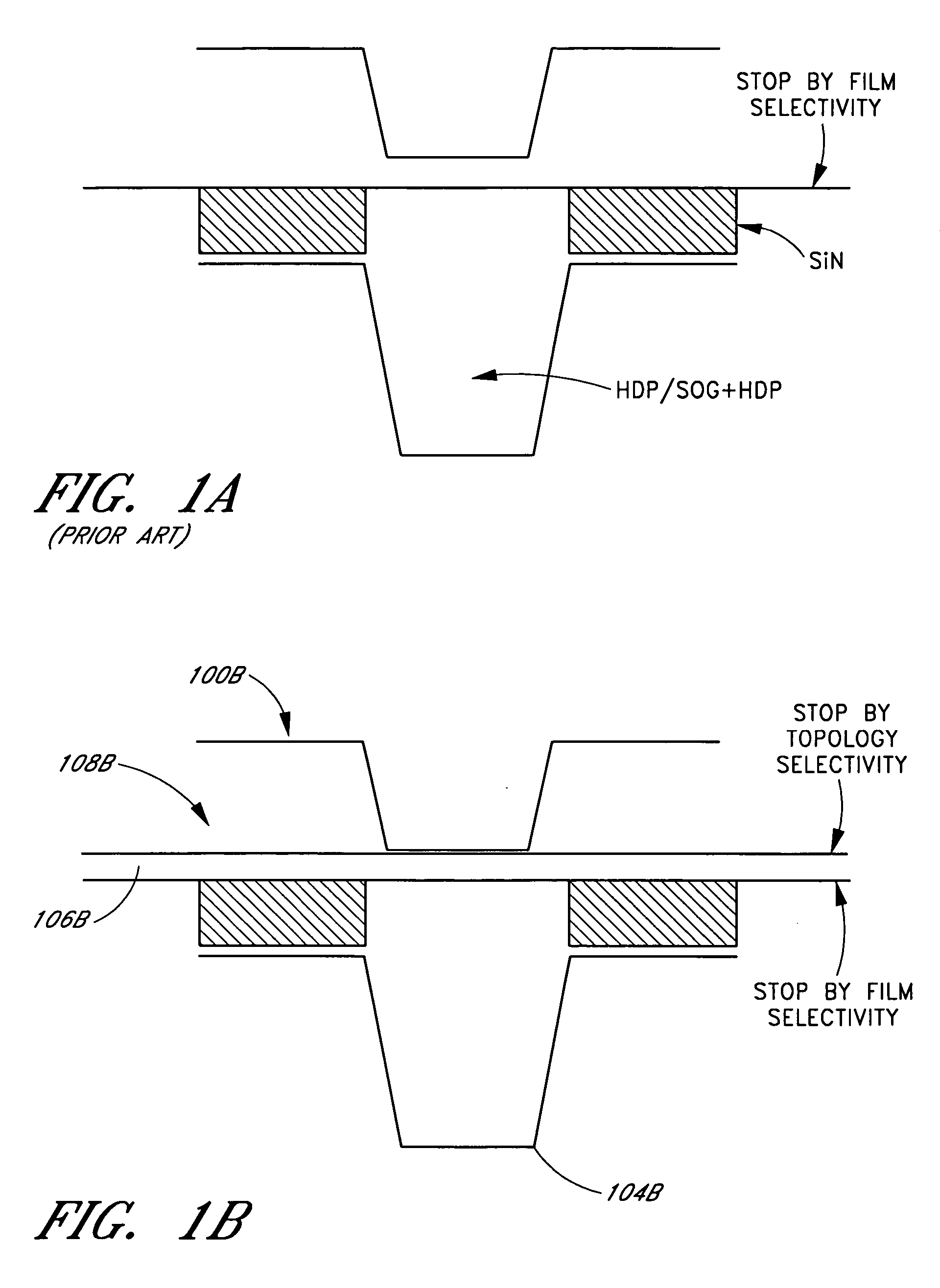
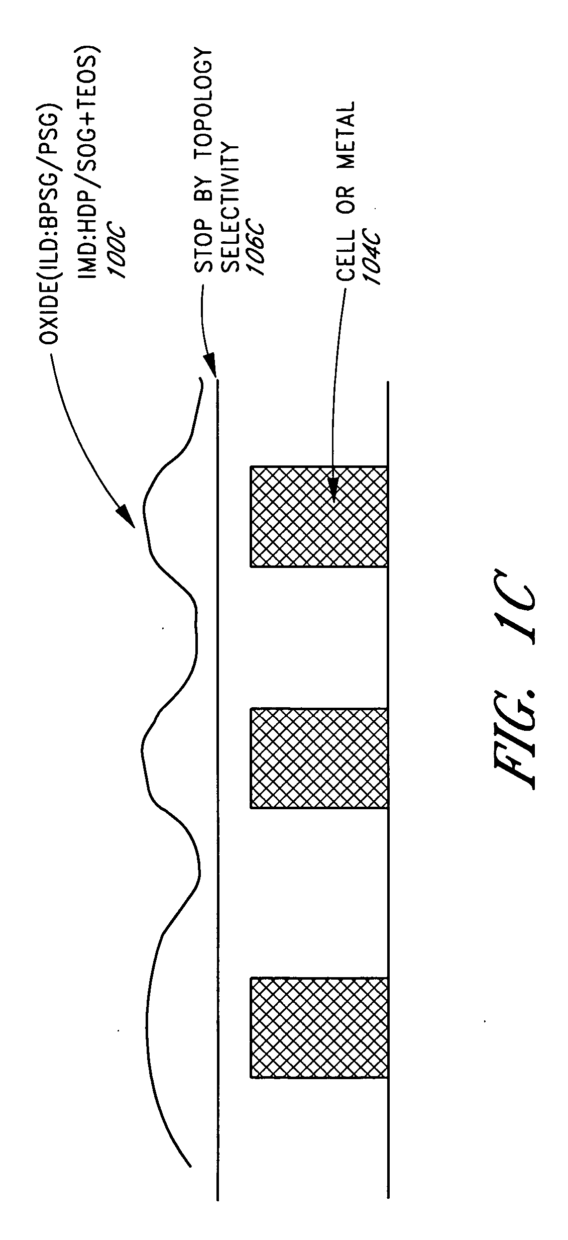
Topology-selective oxide CMP
a topology selectivity and oxide technology, applied in the direction of electrical equipment, decorative surface effects, decorative arts, etc., can solve the problems of poor deposition uniformity of -chamber cvd systems, inconvenient use of conventional cmp processes, and high cost, and achieve low topology selectivity , high down force, low cost
- Summary
- Abstract
- Description
- Claims
- Application Information
AI Technical Summary
Benefits of technology
Problems solved by technology
Method used
Image

Examples
Embodiment Construction
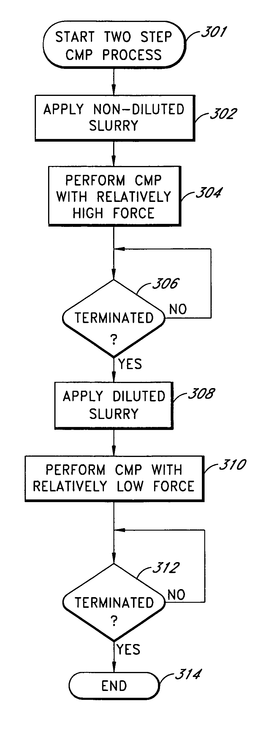
[0020] The present invention relates to chemical mechanical polishing, and in particular to performing chemical mechanical polishing using slurries. Embodiments of the present invention provide topology and / or film selective chemical mechanical polishing that can be used, by way of example, for cell, poly, STI (shallow trench isolation), ILD (Inter-layer dielectric), or IMD (Inter-metal dielectric) polishing.
[0021] In particular, a multi-step CMP process is described wherein a relatively high force, low topology selectivity CMP process is performed first to remove protrusions, and then a relatively low force, high topology selectivity CMP process is performed. The low topology selectivity CMP primarily removes protrusions, while the high topology selectivity CMP is used to achieve a high degree of WIW (With In Wafer) uniformity. For example, a WIW range of 1000 Å or less, or even 500 Å or less, can be achieved using a SAC (self aligned contact) etch process. The topology selective ...
PUM
| Property | Measurement | Unit |
|---|---|---|
| pressure | aaaaa | aaaaa |
| pressure | aaaaa | aaaaa |
| pressure | aaaaa | aaaaa |
Abstract
Description
Claims
Application Information