

Plating method for circuitized substrates
- Summary
- Abstract
- Description
- Claims
- Application Information
AI Technical Summary
Benefits of technology
Problems solved by technology
Method used
Image

Examples
Embodiment Construction
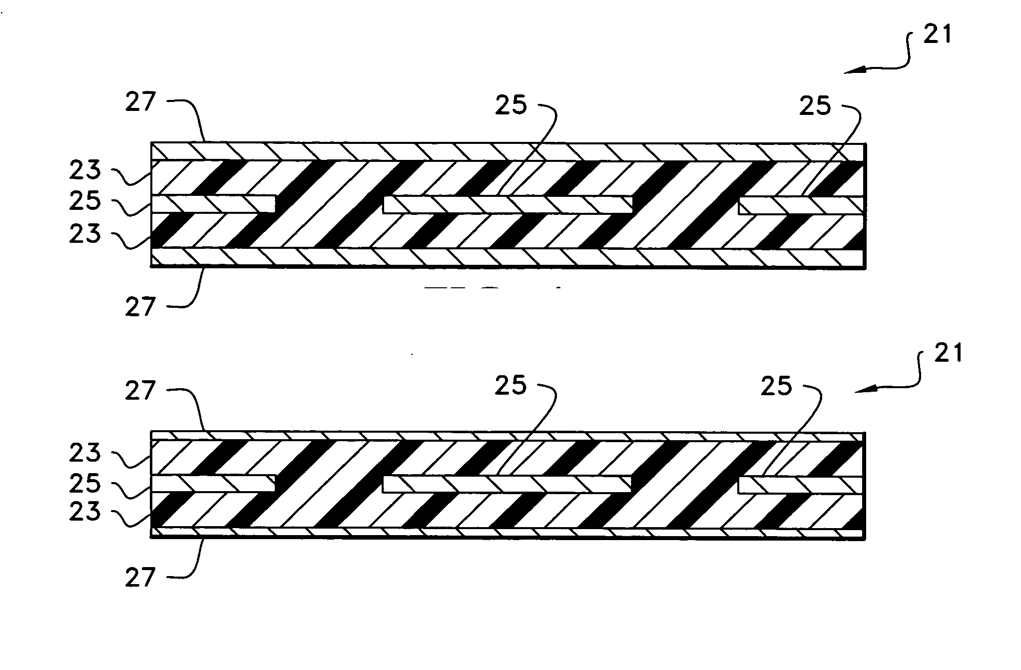
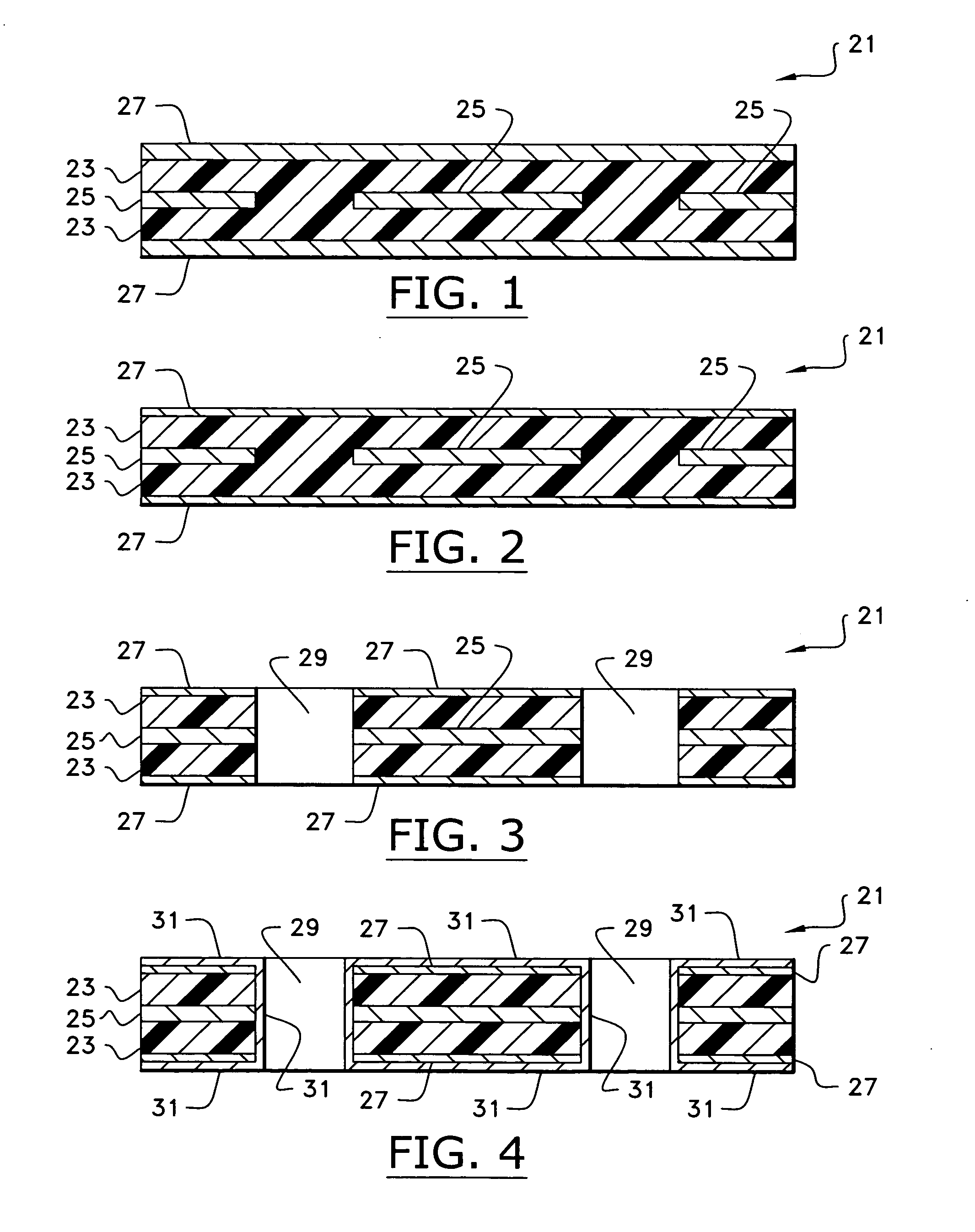
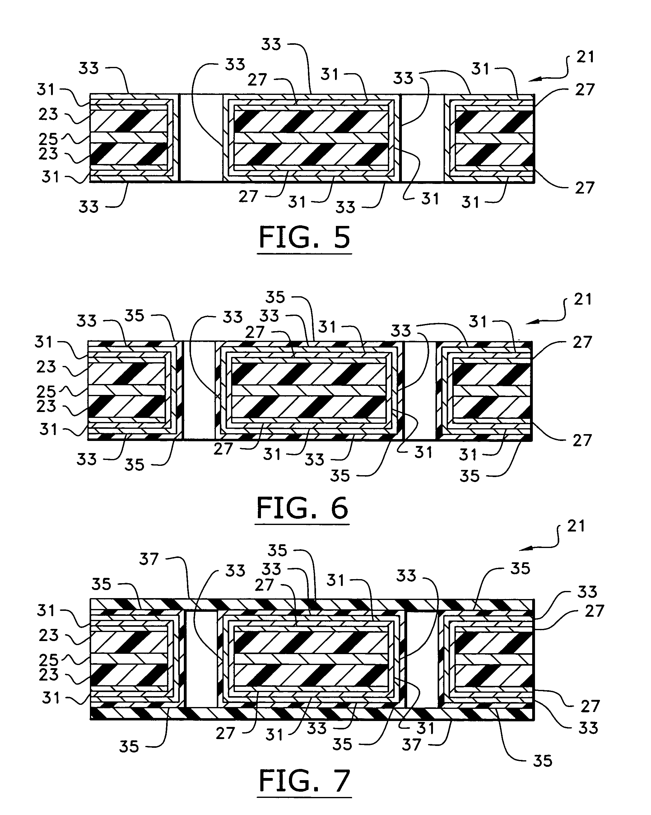
[0025] For a better understanding of the present invention, together with other and further objects, advantages and capabilities thereof, reference is made to the following disclosure and appended claims in connection with the above-described drawings. Like numerals will be used from FIG. to FIG. to reference similar elements.
[0026] By the term “circuitized substrate” as used herein is meant to include substrates having at least one dielectric layer and at least one metallurgical conductive layer. Examples include structures made of dielectric materials such as fiberglass-reinforced epoxy resins (some referred to as “FR-4” dielectric materials in the art), polytetrafluoroethylene (Teflon), polyimides, polyamides, cyanate resins, polyphenylene ether resins, photoimageable materials, and other like materials wherein the conductive layers are each a metal layer (e.g., power, signal and / or ground) comprised of suitable metallurgical materials such as copper (preferably electrodeposited...
PUM
| Property | Measurement | Unit |
|---|---|---|
| Fraction | aaaaa | aaaaa |
| Adhesion strength | aaaaa | aaaaa |
| Electrical conductor | aaaaa | aaaaa |
Abstract
Description
Claims
Application Information