Substrate test apparatus and method of testing substrates

Active Publication Date: 2006-10-31
TTM TECH NORTH AMERICA LLC
View PDF15 Cites 18 Cited by
  • Summary
  • Abstract
  • Description
  • Claims
  • Application Information

AI Technical Summary

Benefits of technology

[0020]It is yet another object of the invention to provide such an apparatus which can be manufactured at relatively low cost and can be operated in a relatively easy manner.
[0021]It is still another object of the invention to provide a method of testing substrates such as test coupons in which the testing can be done in a relatively quick and expeditious manner.

Problems solved by technology

Accordingly, in ATC tests, latent defects in the board will be revealed as the cyclic stressing mechanically exercises any weak or defective element to failure.
Although Mil-T cycling is presently sanctioned by IPC, there are a number of known drawbacks to this approach, particularly for PCB's.
Further, the operation of a Mil-T chamber can be expensive insofar as the chilled portion of the chamber typically relies upon liquid nitrogen, which is costly to ship, store, and use, and which presents certain environmental concerns.
Chamber testing is further limited by the maximum high temperature, which is typically 175C, thus not allowing direct evaluation of assembly temperature cycles from assembly, which are typically at least 220C.
The HATS system is capable of cycling coupons between −60 to 160 degrees C. and achieves faster cycling than conventional chambers due to more efficient exchange between hot and cold air, though the relatively low efficiency of heat transfer in air still limits the actual rate of coupon cycling.
As with other chamber cycle tests, a maximum high temperature of 160 degrees C. limits the range of cycling possible, especially to represent assembly reflow temperatures.
First, direct comparisons of cycle to fail data between cold cycling and reflow cycling on the same coupon design is not possible.
Second, in the common situation where some number of reflow cycles is required as preconditioning prior to a cold cycle stress test, those reflow cycles must be performed in a separate reflow oven.
However, drawbacks of the wet thermal shock are that the cycle is uncontrolled during the hot and cold immersions, so that rate of change is a function of sample mass.
Further, wet thermal shock does not facilitate continuous electrical monitoring during the cycling, and, as with chamber cycling, is also limited to a high temperature of less than 175 degrees C. Another method heats and cools the test coupon by exposing it to a fluidized sand bath.
This method is awkward to use and maintain, and is typically limited to a low temperature of 50 degrees C. Yet another method is referred to as the “Power Cycling Technique” (“PCT”), or, more recently, as “Current Induced Thermal Cycling”.
When the differential expansion causes strain that exceeds the strength of the copper thru-hole plated material, a rupture intermediate the ends of the thru-hole structure may develop due to the thermal stresses generated.
This undesirable occurrence may result in one or more open circuits or intermittent contacts which in turn may lead to failure of the substrate and any system in which it is utilized.
A particular problem associated with such DC voltage thermal testing is the inability to satisfactorily test each coupon across as wide temperature range to which the associated larger substrate will be eventually exposed.
Because many substrates may be required to operate at significantly lower temperatures as well as at much higher temperatures for the lowest operating temperature, testing coupons at ranges where ambient temperature is the only “low” temperature is limited.
Because substrates such as PCBs very often operate at much lower ambient temperatures (e.g., during automotive and military applications), a room temperature ambient as the initial temperature is deemed unsatisfactory to fully evaluate a substrate's end use conditions.

Method used


Image

  • Substrate test apparatus and method of testing substrates
  • Substrate test apparatus and method of testing substrates
  • Substrate test apparatus and method of testing substrates

Examples


Embodiment Construction

[0027]For a better understanding of the present invention, together with other and further objects, advantages and capabilities thereof, reference is made to the following disclosure and appended claims in connection with the above-described drawings. Like figure numbers will be used from FIG. to FIG. to identify like elements in these drawings.

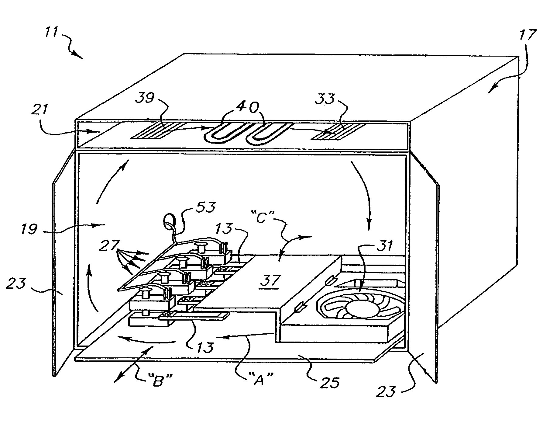
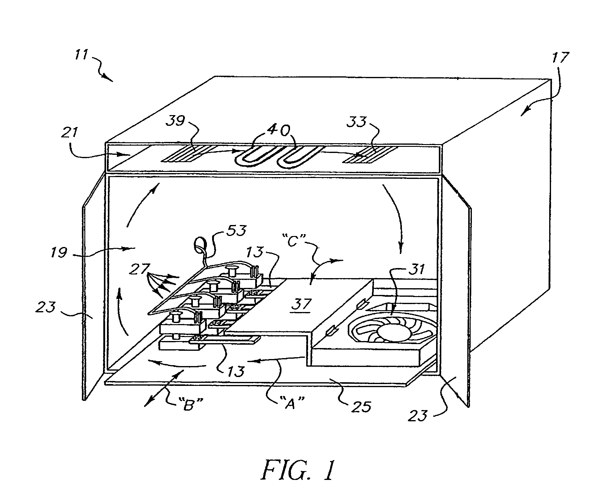
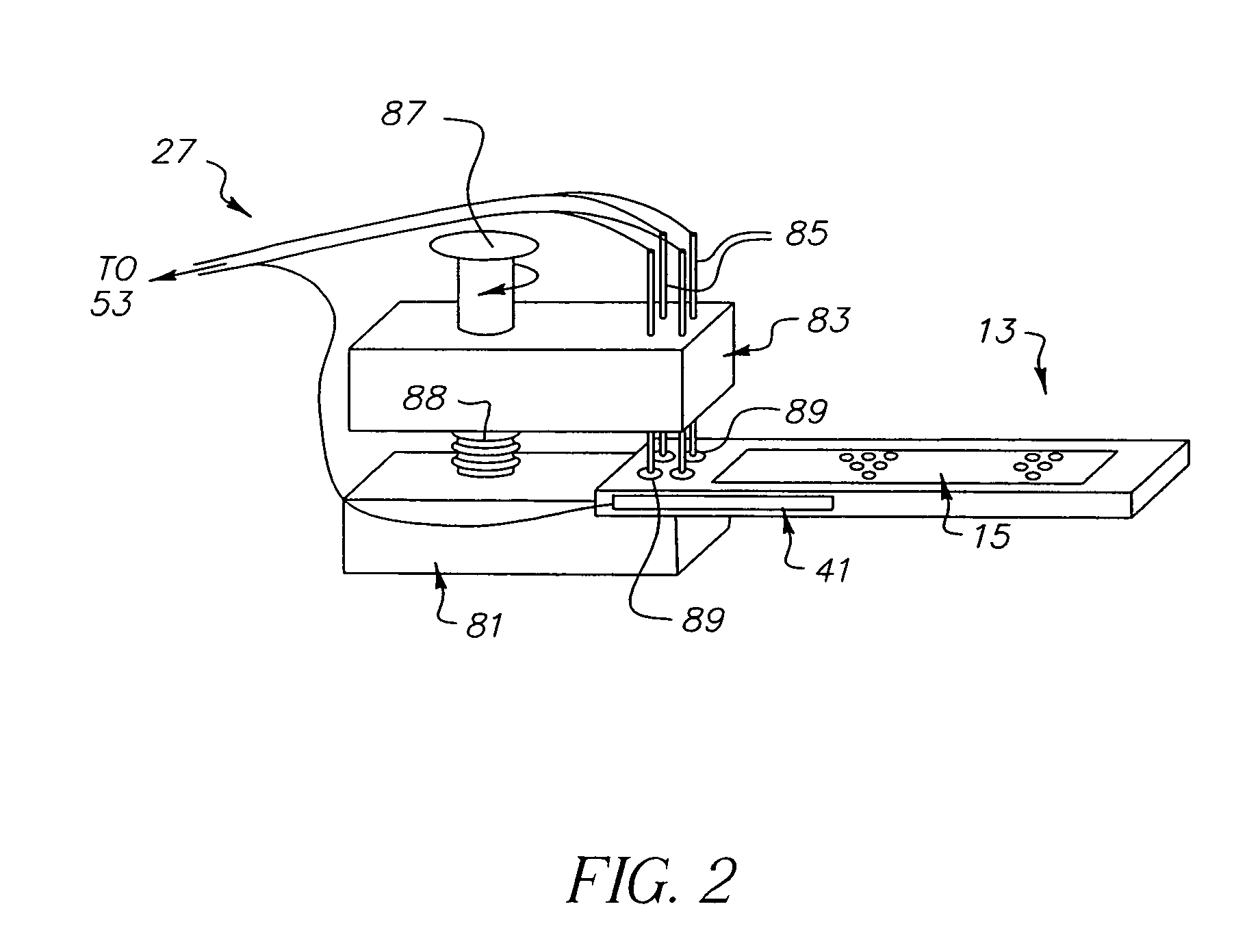
[0028]In FIG. 1 (compare also FIG. 3), there is shown a test apparatus 11 according to one embodiment of the invention. Apparatus 11 is designed for testing at least one (and preferably several, four being shown in FIG. 1) test substrates 13 when positioned therein. In one example, test substrate 13 is a “test coupon” integrally manufactured and processed together with a related, much larger PCB (not shown). Generally speaking, apparatus 11 (and the associated test system described herein-below) tests the coupon by thermally cycling it by first running electric DC current through the daisy-chained thru-holes (located in an area 15 (FIG. 2) bu...


PUM


Abstract

A test apparatus for testing circuitized substrates such as PCB test coupons for thru-hole failure in which the substrate may be cooled to a temperature less than the ambient temperature surrounding the test apparatus housing in which the testing is accomplished. A method of testing substrates is also provided.

Description

TECHNICAL FIELD[0001]This invention relates to test apparatus and particularly to test apparatus for testing circuitized substrates such as test coupons for printed circuit boards and the like products.BACKGROUND OF THE INVENTION[0002]Today's miniaturization requirements for organic circuitized substrates, including multilayered printed circuit boards (PCBs), laminate chip carriers, and the like, require the formation of multiple circuits in a minimum volume or space. These circuits typically comprise a stack of electrically conductive copper or copper alloy layers of signal, ground and / or power planes (lines) separated from each other by a layer of organic dielectric material, typically fiber-glass reinforce resin material known in the art commonly as “FR4.” Selected lines or pads of one conductive layer are often in electrical contact with selected lines and / or pads of other conductive layers using plated holes passing through the dielectric layers. The plated holes are often refe...

Claims


Application Information

Patent Timeline
IPC IPC(8): G01R31/02H05K7/00
CPCG01R31/2817G01R31/2805
Inventor KNADLE, KEVIN T.
Owner TTM TECH NORTH AMERICA LLC
Why Eureka
Try Eureka