Semiconductor device and manufacturing method of the same

Inactive Publication Date: 2006-11-23
RENESAS TECH CORP
View PDF20 Cites 63 Cited by
  • Summary
  • Abstract
  • Description
  • Claims
  • Application Information

AI Technical Summary

Benefits of technology

[0027] Since the power MISFET having the trench gate structure with the dummy gate electrode, and the protective diode are formed on the same semiconductor substrate, the electrostatic breakdown of the gate insulating film can be prevented, while improving the performence of the MISFET.
[0028] The polycrystalline silicon film for the protective diode included in the protective diode, and the polycrystalline silicon film for the dummy gate electro

Problems solved by technology

In the power MISFET having the trench gate structure without any dummy gate electrodes, even if the performance of the MISFET is intended to be enhanced by thinning the gate insulating film, the defective formation of the gate insulating film is likely to oc

Method used


Image

  • Semiconductor device and manufacturing method of the same
  • Semiconductor device and manufacturing method of the same
  • Semiconductor device and manufacturing method of the same

Examples


Embodiment Construction

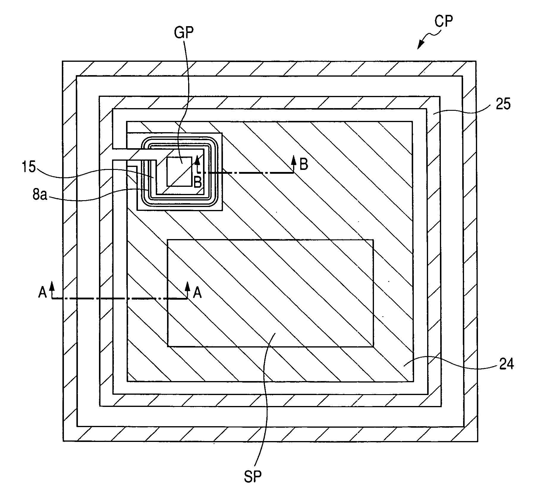
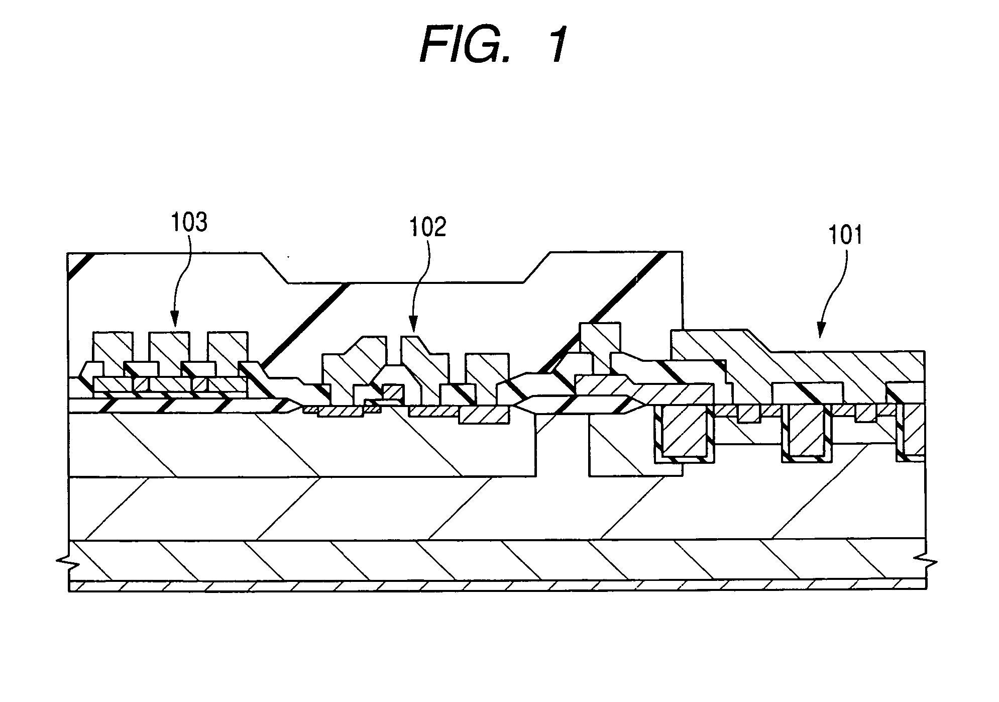
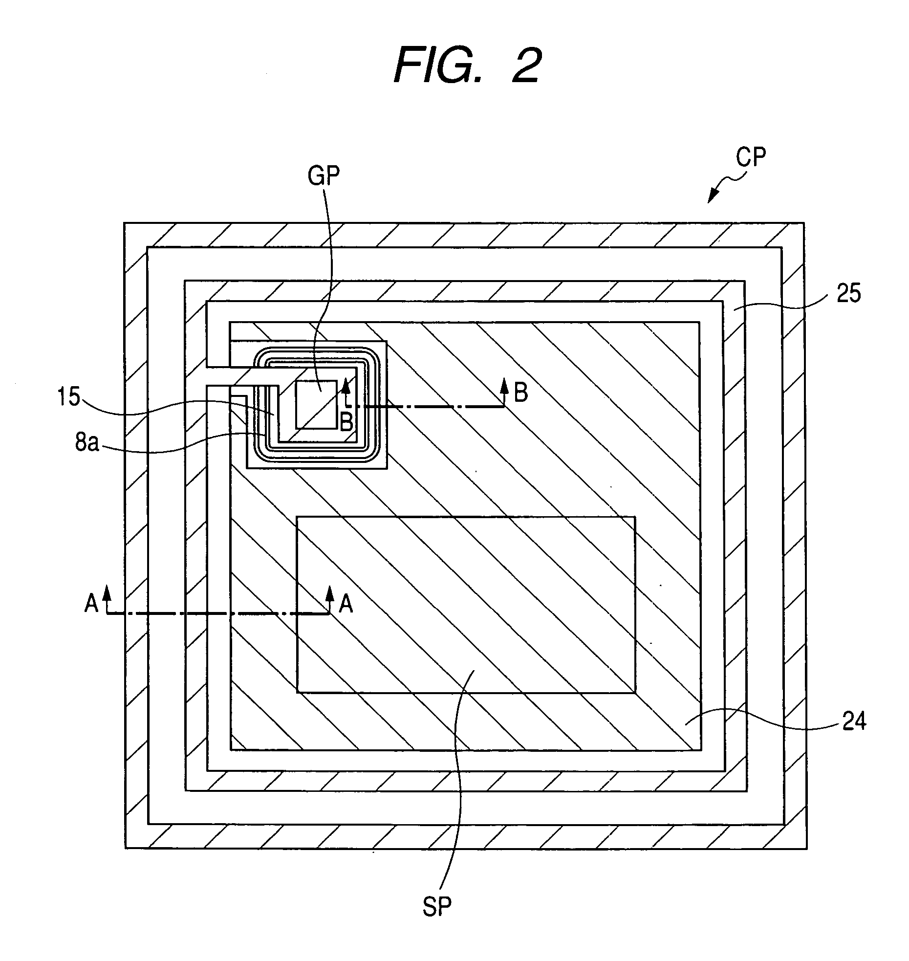
[0054] The following embodiments will be described by being divided into a plurality of sections or embodiments if necessary for convenience. However, unless otherwise specified, they are not irrelevant to one another. One of the embodiments has to do with modifications, details and supplementary explanations of some or all of the other.

[0055] When reference is made to the number of elements or the like (including the number of pieces, numerical values, quantity, range, etc.) in the following description of the embodiments, the number thereof is not limited to a specific number, and may be greater than, or less than, or equal to the specific number, unless otherwise specified and definitely limited to the specific number in principle.

[0056] It is also needless to say that components (including elements or process steps, etc.) employed in the following description of the embodiments are not always essential, unless otherwise specified and considered to be definitely essential in pr...


PUM


Abstract

In a power MISFET having a trench gate structure with a dummy gate electrode, a technique is provided for improving the performance of the power MISFET, while preventing electrostatic breakdown of a gate insulating film therein. A power MISFET having a trench gate structure with a dummy gate electrode, and a protective diode are formed on the same semiconductor substrate. The protective diode is provided between a source electrode and a gate interconnection. In a manufacturing method of such a semiconductor device, a polycrystalline silicon film for the dummy gate electrode and a polycrystalline silicon film for the protective diode are formed simultaneously. A source region of the power MISFET and an n+-type semiconductor region of the protective diode are formed in the same step.

Description

CROSS-REFERENCE TO RELATED APPLICATION [0001] The present application claims priority from Japanese patent application No. 2005-147914 filed on May 20, 2005, the content of which is hereby incorporated by reference into this application. BACKGROUND OF THE INVENTION [0002] The present invention relates to a semiconductor device, and a manufacturing method of the same, and more particularly to a technique suitable for application to a power MISFET (Metal Insulator Semiconductor Field Effect Transistor) having a trench gate structure with a dummy gate electrode, and a manufacturing method of the same. [0003] A patent document 1, as shown in FIG. 1, discloses a structure having a power MISFET 101 with a trench gate structure, a planer gate type MISFET 102, and a protective diode 103 formed on the same substrate. In a method of manufacturing this structure, a polycrystalline silicon film included in a gate electrode of the power MISFET 101, and a polycrystalline silicon film included in ...

Claims


Application Information

Patent Timeline
IPC IPC(8): H01L29/94
CPCH01L27/0255H01L29/0696H01L29/407H01L29/42368H01L29/4238H01L21/28008H01L29/66727H01L29/66734H01L29/7808H01L29/7811H01L29/7813H01L29/456H01L2224/0603H01L21/28556H01L29/4236H01L29/4916H01L29/66484H01L29/66545
Inventor NAKAZAWA, YOSHITOYATSUDA, YUJI
Owner RENESAS TECH CORP
Why Eureka
Try Eureka