Chip package having chip extension and method

a technology of chip and package, applied in the field of chip package, can solve the problems of chip leakage power aggravating, strong influence, “paste pumping”, etc., and achieve the effect of improving heat dissipation

Inactive Publication Date: 2006-11-23
GOOGLE LLC
View PDF14 Cites 53 Cited by
  • Summary
  • Abstract
  • Description
  • Claims
  • Application Information

AI Technical Summary

Benefits of technology

[0012] A third aspect of the invention is related to a method of containing a thermal interface material in a chip package during thermal cycling and improving heat dissipation, the method comprising the steps of: providing a chip extension adjacent to the chip; and placing the thermal interface material between a cooling structure and the chip and the chip extension, whereby the chip extension contains the thermal interface material during thermal cycling and provides a thermal contact area between the cooling structure and the chip.

Problems solved by technology

Chip leakage power is aggravated by shrinking device size, and is strongly affected by operating temperature.
One problem with conventional structures is caused by the relatively high viscosity of high performance thermally conductive pastes.
Unfortunately, the high viscosity also results in “paste pumping,” which refers to the situation in which the TIM is pumped into and out of the gap between chip 10 and cooling structure 18.
These voids 26 have much lower thermal conductivity than TIM 20, causing chip 10 temperature to rise, and further increasing power dissipation, usually because of device leakage current.
These voids 26 tend to grow with additional cycling, further degrading the cooling, degrading device reliability, and increasing the power consumption.
Another problem with conventional structures is that, in most high power flip chip packages, device cooling by heat transfer to and through substrate 12 is nearly negligible.
This chip ‘shrink’ increases the density of the power on the device since the body size is physically smaller for the same power consumption.

Method used


Image

  • Chip package having chip extension and method
  • Chip package having chip extension and method
  • Chip package having chip extension and method

Examples


Embodiment Construction

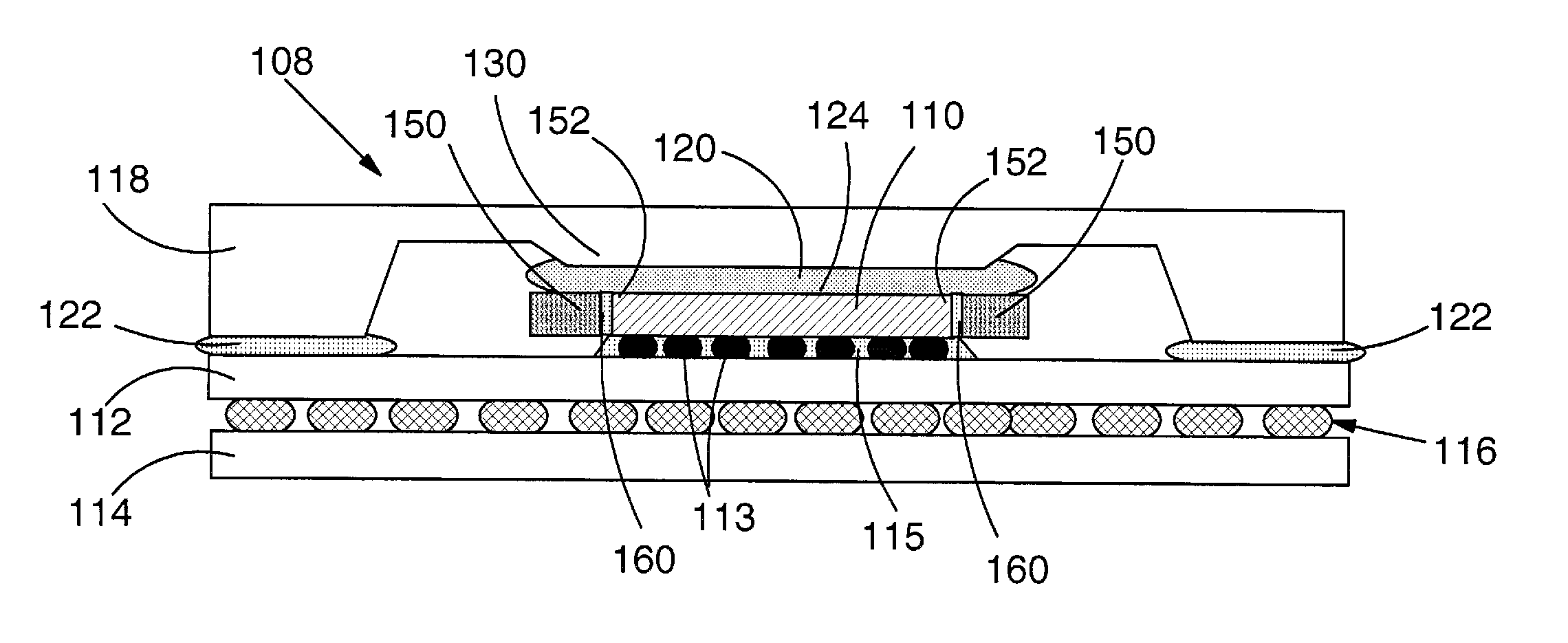
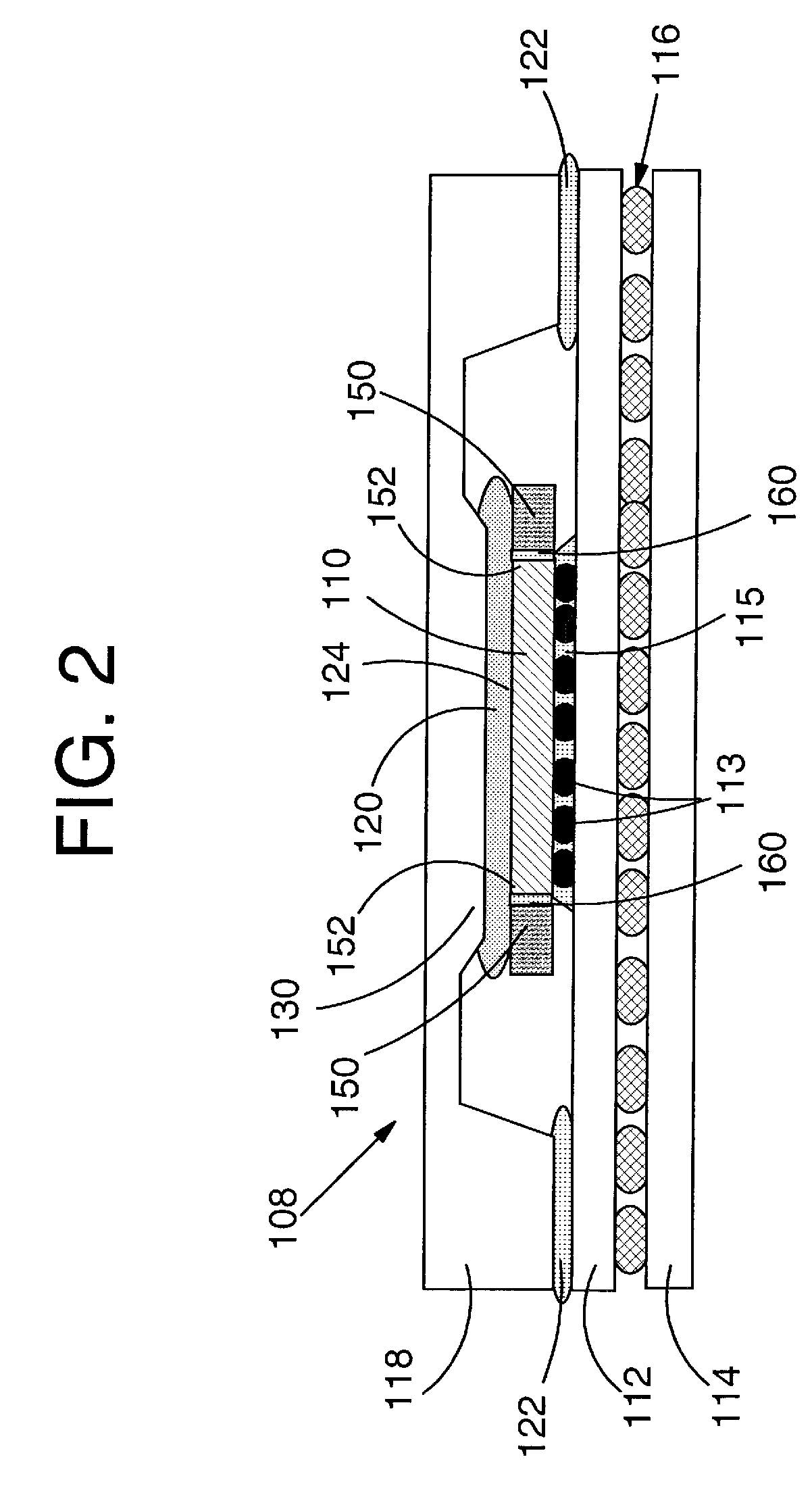
[0020] The invention includes a chip package including a chip extension that contains thermal interface material (TIM) and improves chip cooling, and a related method. With reference to the accompanying drawings, FIG. 2 shows one embodiment of a chip package 108 according to the invention. Chip package 108 includes a chip 110 electrically connected to a substrate 112 by solder connections 113 and under-fill material 115. Substrate 112 is in turn electrically connected to a card 114 via a conventional grid array 116, e.g., ball grid array (BGA), column grid array (CGA), land grid array (LGA) or pin grid array (PGA). A cooling structure 118 is thermally coupled by a TIM 120 to chip 110 to provide a thermal path from the chip to cooling structure 118. TIM 120 may include any now known or later developed thermal interface material such as a thermal paste, liquid, phase change material and other materials. Cooling structure 118 is also coupled to substrate 112 via a conventional adhesive...


PUM


Abstract

A chip package including a chip extension for containing thermal interface material (TIM) and improves chip cooling, and a related method, are disclosed. In particular, the chip package includes a chip, a cooling structure coupled to the chip via a TIM, and a chip extension may be thermally coupled to an outer edge of the chip. A TIM placed between the chip and the cooling structure is contained during thermal cycling by the chip extension such that void formation at the edge of the chip, which can move between the chip and cooling structure, is suppressed. The chip extension also improves lateral heat dissipation by providing a greater thermal contact area between the cooling structure and the chip and, if needed, the substrate at a much lower cost than using larger die with lower production unit output from a wafer.

Description

BACKGROUND OF THE INVENTION [0001] 1. Technical Field [0002] The present invention relates generally to chip packages, and more particularly, to a chip package including a chip extension for containing thermal interface material and improving chip cooling. [0003] 2. Related Art [0004] The drive for increasing chip performance (higher operating frequencies) is resulting in increased chip power, and the reduction of circuit size is increasing chip power density. Chip leakage power is aggravated by shrinking device size, and is strongly affected by operating temperature. As a result, as chips continue to become smaller, there is a need to continue enhancing chip cooling capability. [0005] One common cooling mechanism is to thermally connect chips to a cooling structure, such as a lid or heat sink, via a thermal interface material (TIM). Commonly used TIMs include thermal pastes, thermal adhesives, and phase change materials; and less commonly used TIMs include liquid metals and solders...

Claims


Application Information

Patent Timeline
Patent Type & Authority Applications(United States)
IPC IPC(8): H01L23/34
CPCH01L23/04H01L23/3675H01L2924/01033H01L2924/01006H01L2224/32225H01L2924/16195H01L2924/16152H01L2924/15311H01L2924/01074H01L2924/01047H01L2924/01042H01L2924/01029H01L2924/01027H01L2924/01013H01L2924/01005H01L2224/92125H01L2224/83102H01L23/433H01L24/31H01L2224/16225H01L2224/27013H01L2224/73204H01L2224/73253H01L2224/83051H01L2924/00H01L2924/00012H01L2924/00011H01L2924/00014H01L2224/0401
Inventor COLGAN, EVAN G.EDWARDS, DAVID L.FASANO, BENJAMIN V.SIKKA, KAMAL K.ZITZ, JEFFREY A.ZOU, WEI
Owner GOOGLE LLC
Why Eureka
Try Eureka