Semiconductor device and method for manufacturing the same

Inactive Publication Date: 2006-11-23
KK TOSHIBA
View PDF28 Cites 22 Cited by
  • Summary
  • Abstract
  • Description
  • Claims
  • Application Information

AI Technical Summary

Benefits of technology

[0015] According to still another aspect of the present invention, it is provided a method for manufacturing a semiconductor device, comprising: depositing a first insulator above a semiconductor substrate; forming at least one of a wiring trench and contact hole in the first insulator; recovering damage introduced to the first insulator in the vicinity of the surface of the wiring trench and / or contact hole; forming a second insulator on a surface of the wiring trench and / or contact hole; forming a barrier metal on the second insulator; and forming a conductive layer in at least one of the wiring trench and contact hole.

Problems solved by technology

However, following problems arise if it is desired to form a high performance and reliable multilevel interconnect structure using the porous low k insulator.
(2) In forming wiring trenches (slit) and contact holes, the insulator receives plasma damage caused by, such as, reactive ion etching and plasma ashing.
As a result, an increase in resistance of contact plug and / or open in the interconnect structure could occur, therefore, there is a problem that performance and reliability of the interconnect structure are degraded.
Besides, the following have been known as typical problems of the porous low k insulator, such as, reduction in adhesivity between the low k insulator and silicon oxide film (SiO2 film), peeling of the SiO2 film, corrosion of wiring materials, and diffusion of barrier metal elements to the low k insulator, and the like.
Thus, the treatment does not contribute for preventing corrosion of a barrier metal formed inside of the contact hole and wiring trench.
However, the treatment is not sufficient enough to prevent corrosion of barrier metal and wiring material.
However, the technique does not describe about recovery of damage introduced to the low k insulator and diffusion of moisture absorbed in the damaged layer to the barrier metal.

Method used


Image

  • Semiconductor device and method for manufacturing the same
  • Semiconductor device and method for manufacturing the same
  • Semiconductor device and method for manufacturing the same

Examples


first embodiment

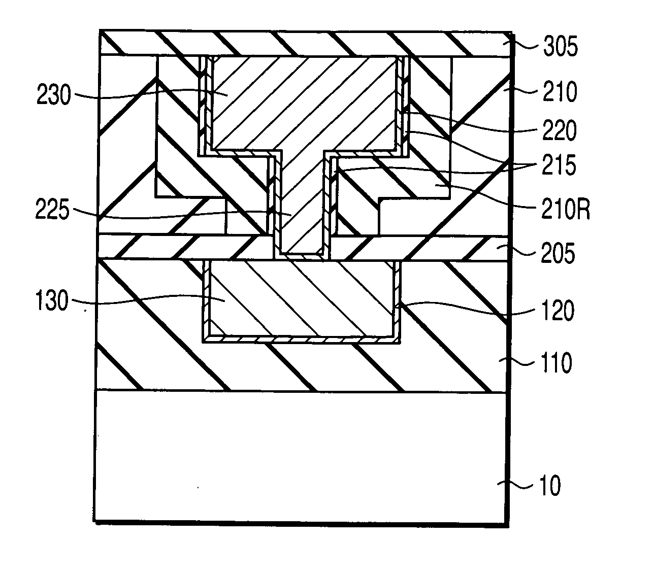
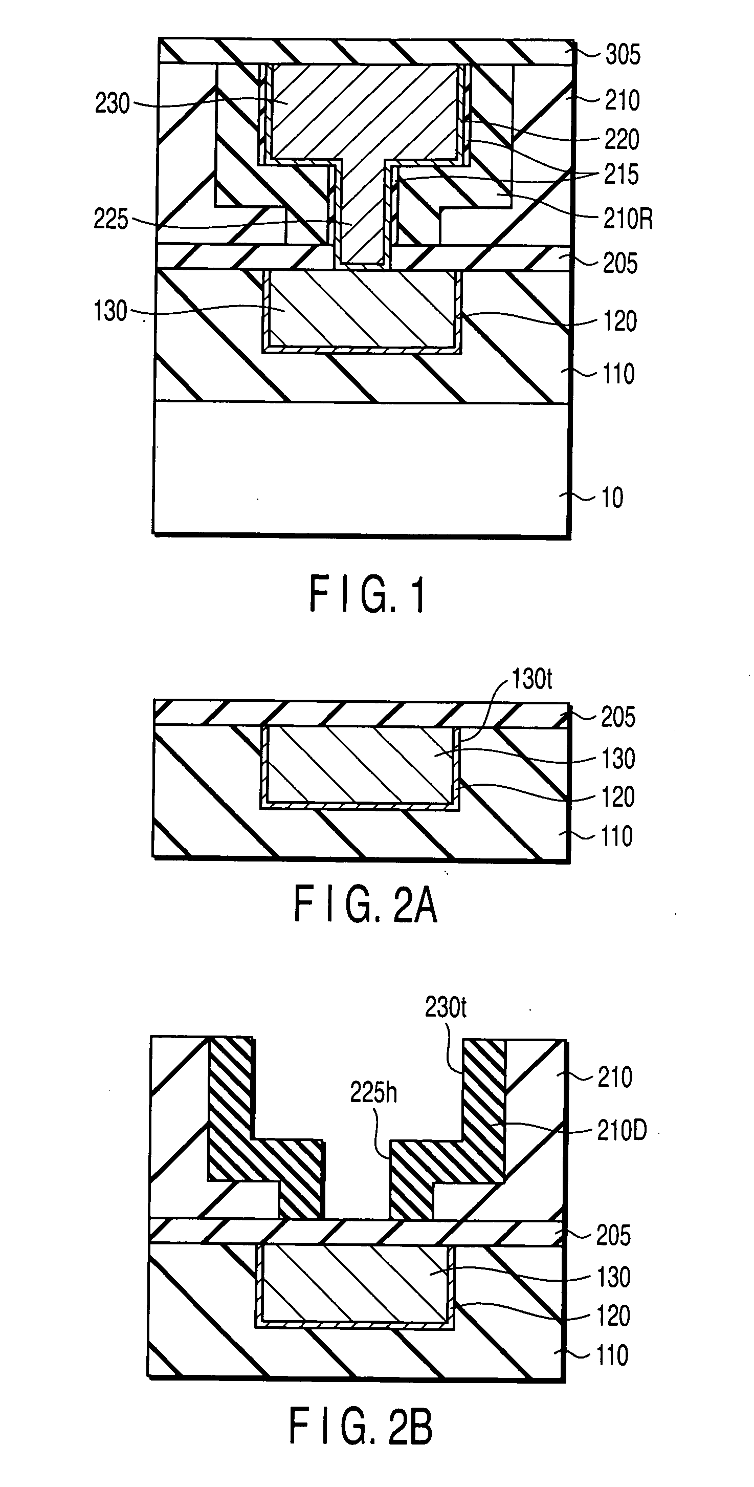
[0028]FIG. 1 shows an example of a sectional structure of a semiconductor device according to a first embodiment of the present invention. The first embodiment relates to a semiconductor device comprising: a second interlevel insulator 210 formed above a semiconductor substrate 10; a recovered layer 210R in which damages introduced to the etched surface of wiring trench and contact hole during their formation are recovered by using an organic material; and a contact plug 225 and a second wiring 230 formed on the recovered layer 210R through a second insulator 215 and second barrier metal 220, and to a method for manufacturing the same.

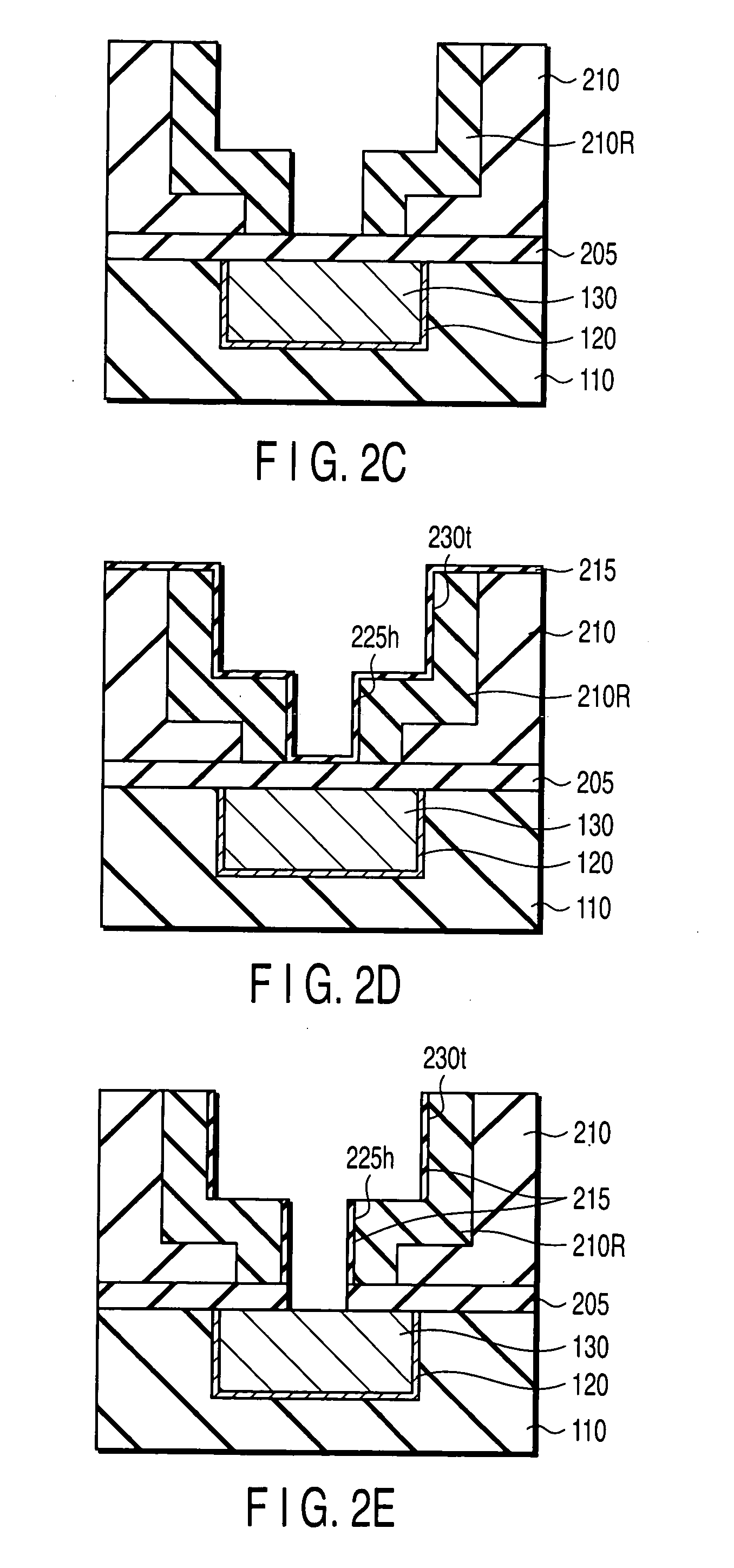
[0029] An example of a manufacturing process the semiconductor device according to the first embodiment will be explained below with reference to cross-sectional views shown in FIG. 2A to FIG. 2F. In the following FIG. 2A to FIG. 2F, the semiconductor substrate is omitted, and an interconnect structure which is directly related to the present inventio...

second embodiment

[0042] The second embodiment of the present invention relates to a semiconductor device comprising features that a first diffusion preventing film 205 on a first wiring 130 at the bottom of a contact hole 225h is removed first, then damage introduced to a second interlevel insulator 210 during its etching is recovered. Thereby, the reliability of contact plug and wiring is improved. According to the second embodiment, damage introduced to the bottom of the second wiring trench 230t is further reduced as compared with the first embodiment.

[0043] The manufacturing process of the semiconductor device according to the second embodiment will be explained below with reference to cross-sectional views shown in FIG. 3A to FIG. 3C.

[0044] (1) As shown in FIG. 3A, a first wiring 130 is formed in a first insulator 110. A first diffusion preventing film 205 and second interlevel insulator 210 are formed on the surface of the first insulator 110 and first wiring 130. Then a contact hole 225h an...

third embodiment

[0051] The third embodiment of the present invention relates to a semiconductor device and a method for manufacturing the same, in which damage introduced in the vicinity of a contact hole is recovered. A contact plug is one of the most damage sensitive portion where the degradation in the reliability of the interconnect structure is easy to occur. Here, only contact hole is first formed in a low k interlevel insulator, and then, a wiring trench is formed after damaged layer in the interlevel insulator around the contact hole is recovered.

[0052] The process of manufacturing the semiconductor device according to the third embodiment will be described below with reference to sectional views shown in FIG. 4A to FIG. 4D.

[0053] (1) As shown in FIG. 4A, a first wiring 130 is formed in a first insulator 110. Then, a first diffusion preventing film 205 and second interlevel insulator 210 are formed on the surface of the first insulator 110 and first wiring 130. A contact hole 225h is form...


PUM


Abstract

A semiconductor device and a method for manufacturing the same, in which degradation of performance of the interconnect structure caused by damage introduced to the low k interlevel insulator is suppressed, is disclosed. The semiconductor device comprises a low dielectric constant insulator formed with at least one of a wiring trench and contact hole therein and including a recovered layer in the vicinity of a surface of the wiring trench and / or contact hole by treating to make a carbon concentration and / or film density therein being equal to or higher than those in the inside of the insulator, a conductive layer formed in the wiring trench and / or contact hole, a barrier metal interposed between the low dielectric constant insulator and the conductive layer, and a second insulator interposed between the barrier metal and the low dielectric constant insulator.

Description

CROSS-REFERENCE TO RELATED APPLICATIONS [0001] This application is based upon and claims the benefit of priority from prior Japanese Patent Application No. 2005-145575, filed May 18, 2005, the entire contents of which are incorporated herein by reference. BACKGROUND OF THE INVENTION [0002] 1. Field of the Invention [0003] The present invention relates to a semiconductor device, and to a method for manufacturing the same. In particular, the present invention relates to a semiconductor device using a low dielectric constant insulator for an interlevel insulator, and to a method for manufacturing the same. [0004] 2. Description of the Related Art [0005] As scale-down and high integration of semiconductor devices progress, a low dielectric constant (hereinafter, referred to as low k) insulator is widely employed as an interlevel insulator to suppress an increase in parasitic capacitance of interconnect and to achieve higher speed operation. In order to obtain such a low k insulator, for...

Claims


Application Information

Patent Timeline
IPC IPC(8): H01L23/52
CPCH01L21/76808H01L21/76826H01L21/76831H01L21/76849H01L23/5222H01L2924/0002H01L23/5226H01L23/53295H01L2924/00
Inventor TSUMURA, KAZUMICHINAKAMURA, NAOFUMI
Owner KK TOSHIBA
Why Eureka
Try Eureka