Semiconductor device and method for manufacturing the same

a semiconductor and semiconductor technology, applied in the field of semiconductor devices, can solve the problems of high manufacturing cost, high manufacturing cost, and all bare chips will be determined to be defective, and achieve the effect of preventing separation or cracking and increasing the yield rate of semiconductor devices

Inactive Publication Date: 2006-11-23
ALPS ALPINE CO LTD
View PDF12 Cites 18 Cited by
  • Summary
  • Abstract
  • Description
  • Claims
  • Application Information

AI Technical Summary

Benefits of technology

[0028] According to the present invention, even in a case where the positional relationship between the elastic contacts and the electrodes is subject to relative displacement caused by a difference in coefficient of thermal expansion, the elastic contacts can be slid against the electrodes so as to be continuously elastically biased against the electrodes. Accordingly, this prevents separation or cracking in the electrode connection areas, whereby the electrical connection between the elastic contacts and the electrodes can be properly maintained.
[0029] Furthermore, since the matching inspection is incorporated into the manufacturing process, a combination of mismatched electronic components is prevented before the electronic components are fixedly bonded to each other. Accordingly, this contributes to a higher yield rate of the semiconductor device, which is the end product.

Problems solved by technology

Therefore, even in a case where only some of the bare chips are mismatched, all of the bare chips will be determined to be defective.
This is problematic in that the yield rate is lowered, thus resulting in high manufacturing costs.
However, a process for separating at least one of the bare chips from the other bare chips, which are physically connected to each other with, for example, wires or electrically conductive adhesives, is extremely complicated, and thus leads to high manufacturing costs.
Therefore, even though the invention set forth in Japanese Unexamined Patent Application Publication No. 11-274375 may be theoretically correct, the semiconductor device according to such an invention is impractical and is actually difficult to manufacture.

Method used


Image

  • Semiconductor device and method for manufacturing the same
  • Semiconductor device and method for manufacturing the same
  • Semiconductor device and method for manufacturing the same

Examples


first embodiment

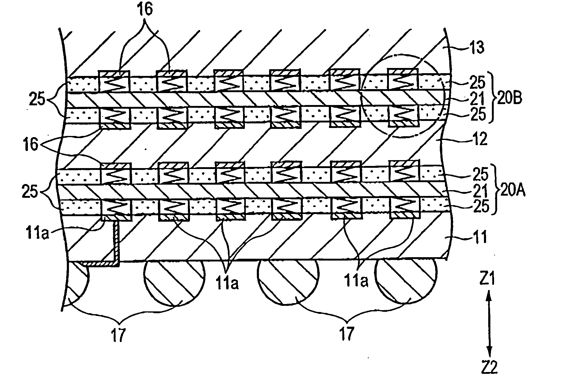
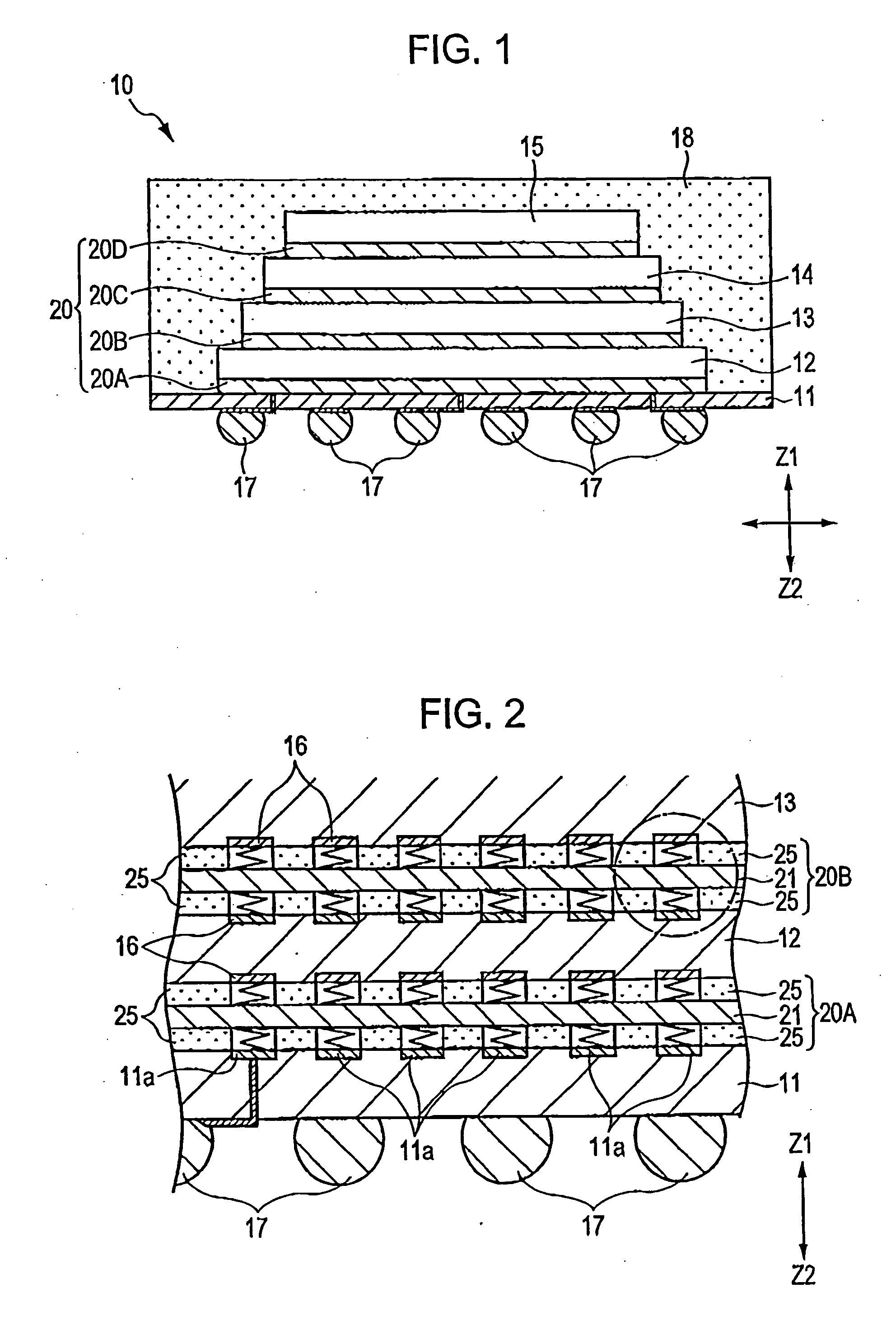
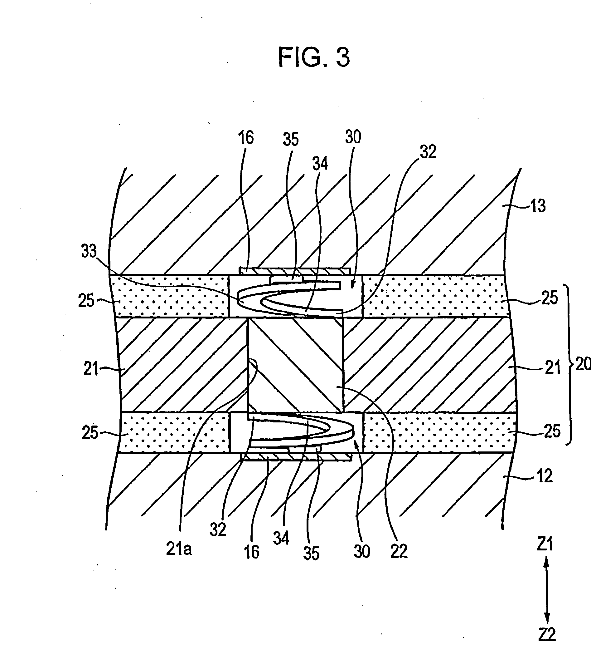
[0037]FIG. 1 is a cross-sectional view of a semiconductor device 10 according to an exemplary embodiment of the present invention. FIG. 2 is an enlarged cross-sectional view of a relevant portion of FIG. 1. FIG. 3 is a cross-sectional view of a relevant portion of FIG. 2 and shows spiral contact members according to the present invention. FIG. 4 is a partially enlarged view corresponding to FIG. 3 and shows a state of thermal expansion.

[0038] The semiconductor device 10 shown in FIG. 1 is packaged in a single unit, and is provided with a base substrate 11 at the bottommost position of the device 10 in a direction of an arrow Z2. The semiconductor device 10 has a multilayer structure in which a plurality of electronic components 12, 13, 14, 15, such as semiconductor bare chips (which will be referred to as bare chips hereinafter), are stacked one on top of the other above the base substrate 11 in a height direction (Z) of the device 10.

[0039] Referring to FIG. 2, at least one of upp...

second embodiment

[0053] the present invention will now be described with reference to FIG. 5.

[0054]FIG. 5 is a partial cross-sectional view similar to FIG. 3 and illustrates stressed metal members according to the second embodiment of the present invention.

[0055] The second embodiment shown in FIG. 5 is directed to an example in which stressed metal members 40 are used as the elastic contacts 30. Other configurations in the second embodiment are substantially the same as those in the first embodiment.

[0056] Each of the stressed metal members 40 includes a bent conductive contact strip 41. The contact strip 41 has a stationary portion 41a and an elastically deformable portion 41b. One of the surfaces of the stationary portion 41a is provided with a sacrificial layer 42. The sacrificial layer 42 may either be conductive or insulative. For example, the sacrificial layer 42 may be, for example, a resin layer mixed with Ti or conductive filler.

[0057] The contact strip 41 is coated with a conductive me...


PUM


Abstract

The present invention relates to a semiconductor device and a method for manufacturing the same that prevent deformation or cracking caused by a difference in coefficient of thermal expansion. Elastic contacts provided on upper and lower surfaces of an interposer are elastically biased against the relatively displaced electrodes. The interposer thus compensates for displacement caused by different coefficients of thermal expansion so that an electrical connection between the electrodes of the first electronic component and the electrodes of the second electronic component is constantly maintained. Accordingly, this prevents separation or cracking in electrode connection areas.

Description

BACKGROUND OF THE INVENTION [0001] 1. Field of the Invention [0002] The present invention relates to semiconductor devices and methods for manufacturing the same. In particular, the present invention relates to a semiconductor device and a method for manufacturing the same that prevent deformation or cracking caused by a difference in coefficient of thermal expansion so as to ensure a proper electrical connection between electronic components or between an electronic component and a base substrate. [0003] 2. Description of the Related Art [0004] In the field of semiconductor devices in recent years, a technology of densification is developing by means of stacking a plurality of bare chips (electronic components) in a single package. There are several known packaging techniques for connecting electrodes of the plurality of bare chips to electrodes of a base substrate on which the bare chips are mounted. For example, such packaging techniques include a wire-bonding packaging technique...

Claims


Application Information

Patent Timeline
Patent Type & Authority Applications(United States)
IPC IPC(8): H01L23/52
CPCH01L2924/3011H01L2924/01006H01L24/72H01L25/0657H01L2225/06517H01L2225/06527H01L2225/06541H01L2225/06593H01L2225/06596H01L2924/01015H01L2924/01029H01L2924/01033H01L2924/01075H01L2924/01078H01L2924/01079H01L2924/12044H01L2924/15311H01L23/3128H01L2924/351H01L2924/181H01L2924/00
Inventor SOETA, KAORUTAKAI, DAISUKE
Owner ALPS ALPINE CO LTD
Why Eureka
Try Eureka