Electronic substrate manufacturing method, semiconductor device manufacturing method, and electronic equipment manufacturing method

a manufacturing method and semiconductor technology, applied in the direction of conductive pattern formation, sustainable manufacturing/processing, final product manufacturing, etc., can solve the problems of reducing productivity, increasing costs, and difficult to reduce thickness and density

Inactive Publication Date: 2006-11-23
SEIKO EPSON CORP
View PDF29 Cites 31 Cited by
  • Summary
  • Abstract
  • Description
  • Claims
  • Application Information

AI Technical Summary

Benefits of technology

[0029] Hence in this invention, the substrate is bonded directly to the housing, so that electronic equipment which is more thin and compact can be manufactured.

Problems solved by technology

In the technology of Patent Literature 1, electronic components are mounted on a substrate material having copper wiring, so that reduction of thickness and increases in density have been difficult.
In the technology of Patent Literature 2, it is necessary to separately prepare an electrical insulation sheet on which conductive paste is formed at positions corresponding to the external connection electrodes of the electronic components, possibly resulting in increased costs and lowered productivity.

Method used


Image

  • Electronic substrate manufacturing method, semiconductor device manufacturing method, and electronic equipment manufacturing method
  • Electronic substrate manufacturing method, semiconductor device manufacturing method, and electronic equipment manufacturing method
  • Electronic substrate manufacturing method, semiconductor device manufacturing method, and electronic equipment manufacturing method

Examples


Embodiment Construction

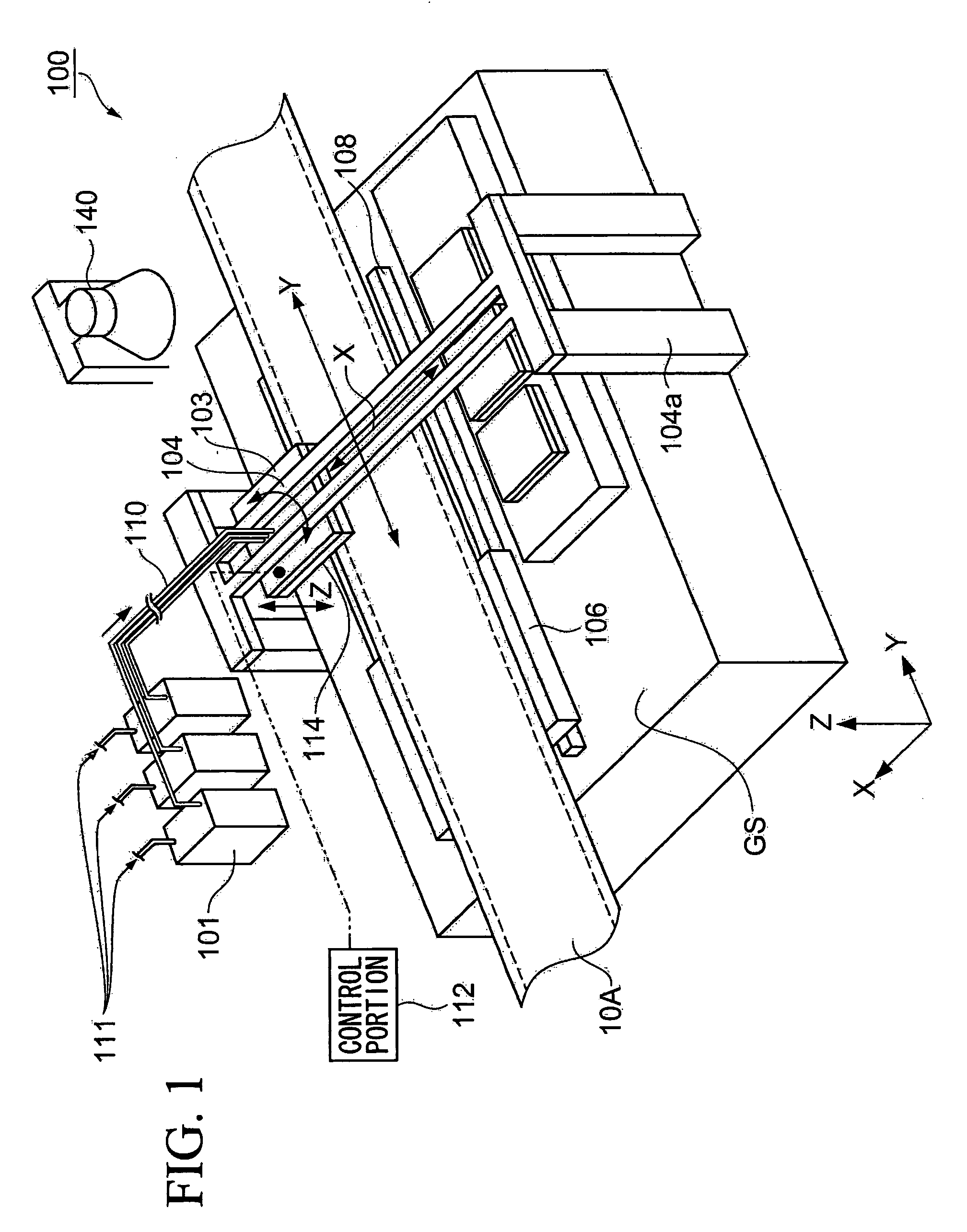
[0038] Below, embodiments of an electronic substrate manufacturing method, semiconductor device manufacturing method, and electronic equipment manufacturing method of this invention are explained, referring to FIGS. 1 to 8.

[0039] Liquid Droplet Ejection Device

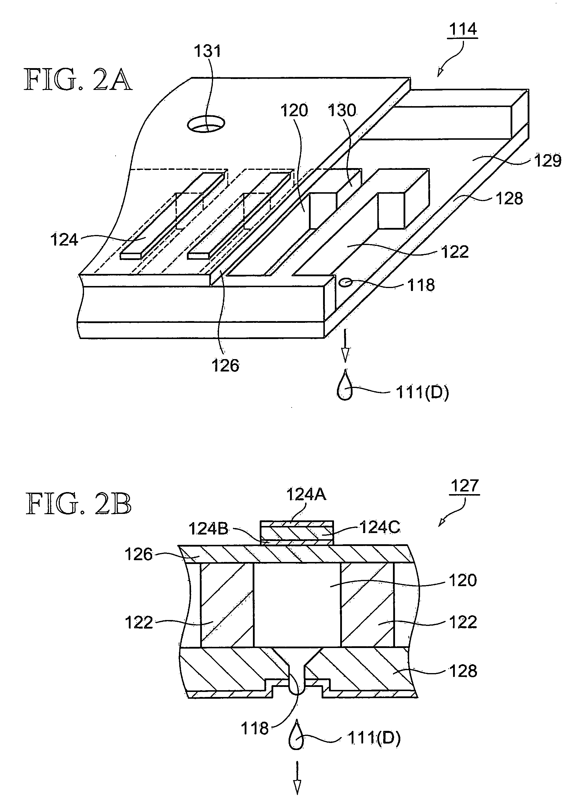
[0040] First, a liquid droplet ejection device used in the manufacture of an electronic substrate, semiconductor device, and electronic equipment is explained, referring to FIGS. 1, 2A, and 2B.

[0041] The liquid droplet ejection device 100 shown in FIG. 1 is, in essence, an inkjet device. More specifically, the liquid droplet ejection device 100 has a tank 101 which holds liquid material 111, a tube 110, a grand stage GS, a ejection head portion 103, a stage 106, a first position control device 104, a second position control device 108, a control portion 112, a light irradiation device 140, and a support portion 104a.

[0042] The ejection head portion 103 holds the head 114 (see FIGS. 2A and 2B). The head 114 ejects liquid dro...


PUM


Abstract

A method of manufacture of an electronic substrate, having a process of embedding electronic components in a substrate, and a process of ejecting liquid droplets containing a conductive material, to form a wiring pattern connected to the external connection electrodes of the electronic components embedded in the substrate.

Description

CROSS-REFERENCE TO RELATED APPLICATION [0001] This application claims priority to Japanese Patent Application No. 2005-149097, filed May 23, 2005, the contents of which are incorporated herein by reference. BACKGROUND [0002] 1. Technical Field [0003] This invention relates to an electronic substrate manufacturing method, a semiconductor device manufacturing method, and an electronic equipment manufacturing method. [0004] 2. Related Art [0005] With the enhanced performance and increasing compactness of electronic equipment in recent years, there have been demands for electronic substrates for electronic component mounting with ever-higher densities and greater functionality. For example, Japanese Unexamined Patent Application, First Publication No. H03-69191 (Patent Literature 1) discloses technology in which electronic components are mounted on copper wiring formed on the substrate, an electronic component embedding layer of resin is formed to cover the components all at once, and b...

Claims


Application Information

Patent Timeline
Patent Type & Authority Applications(United States)
IPC IPC(8): H01L21/00H01L21/84
CPCH01L23/49816H01L2224/0401H01L23/5389H01L24/24H01L24/82H01L25/0652H01L25/16H01L2224/24227H01L2224/76155H01L2924/01013H01L2924/01015H01L2924/01027H01L2924/01029H01L2924/0103H01L2924/01033H01L2924/01046H01L2924/01049H01L2924/01073H01L2924/01074H01L2924/01077H01L2924/01078H01L2924/01079H01L2924/01082H01L2924/15311H01L2924/19041H01L2924/19042H01L2924/19043H01L2924/19105H01L2924/19106H01L2924/30107H05K1/036H05K1/185H05K3/125H05K3/4664H05K2201/10636H05K2201/10674H05K2203/013H05K2203/1469H01L2924/01005H01L2924/01006H01L2924/01019H01L2924/01024H01L2924/01044H01L2924/01045H01L2924/01047H01L2924/01076H01L2924/014H01L2224/82102H01L2224/04105H01L2224/12105H01L2224/16225H01L2224/24195H01L2224/73267H01L23/49883H01L21/568Y02P70/50H05K3/12
Inventor ITO, HARUKI
Owner SEIKO EPSON CORP
Why Eureka
Try Eureka