
Reaction system for growing a thin film

a technology of reaction system and thin film, which is applied in the direction of crystal growth process, chemically reactive gas, coating, etc., can solve the problems of increased particle emissions, difficult purging of dead pockets and/or recirculation cells, and growth of cvd within the reaction chamber and on the substrate itself, so as to achieve easy purging and eliminate or significantly reduce dead pockets

Active Publication Date: 2006-11-30
ASM IP HLDG BV
View PDF6 Cites 431 Cited by
  • Summary
  • Abstract
  • Description
  • Claims
  • Application Information

AI Technical Summary

Benefits of technology

[0009] A need therefore exists for an improved reactor design which is easier to purge and eliminates or significantly reduces dead pockets in which reactants may remain after a purging step.

Problems solved by technology

In particular, experimental studies have indicated that within the reactor chamber there are dead pockets and / or recirculation cells that are difficult to purge.
This may disadvantageously lead to CVD growth within the reaction chamber and on the substrate itself.
CVD growth within the reaction chamber may disadvantageously lead to increased particle emissions.

Method used


Image

  • Reaction system for growing a thin film
  • Reaction system for growing a thin film
  • Reaction system for growing a thin film

Examples


Embodiment Construction

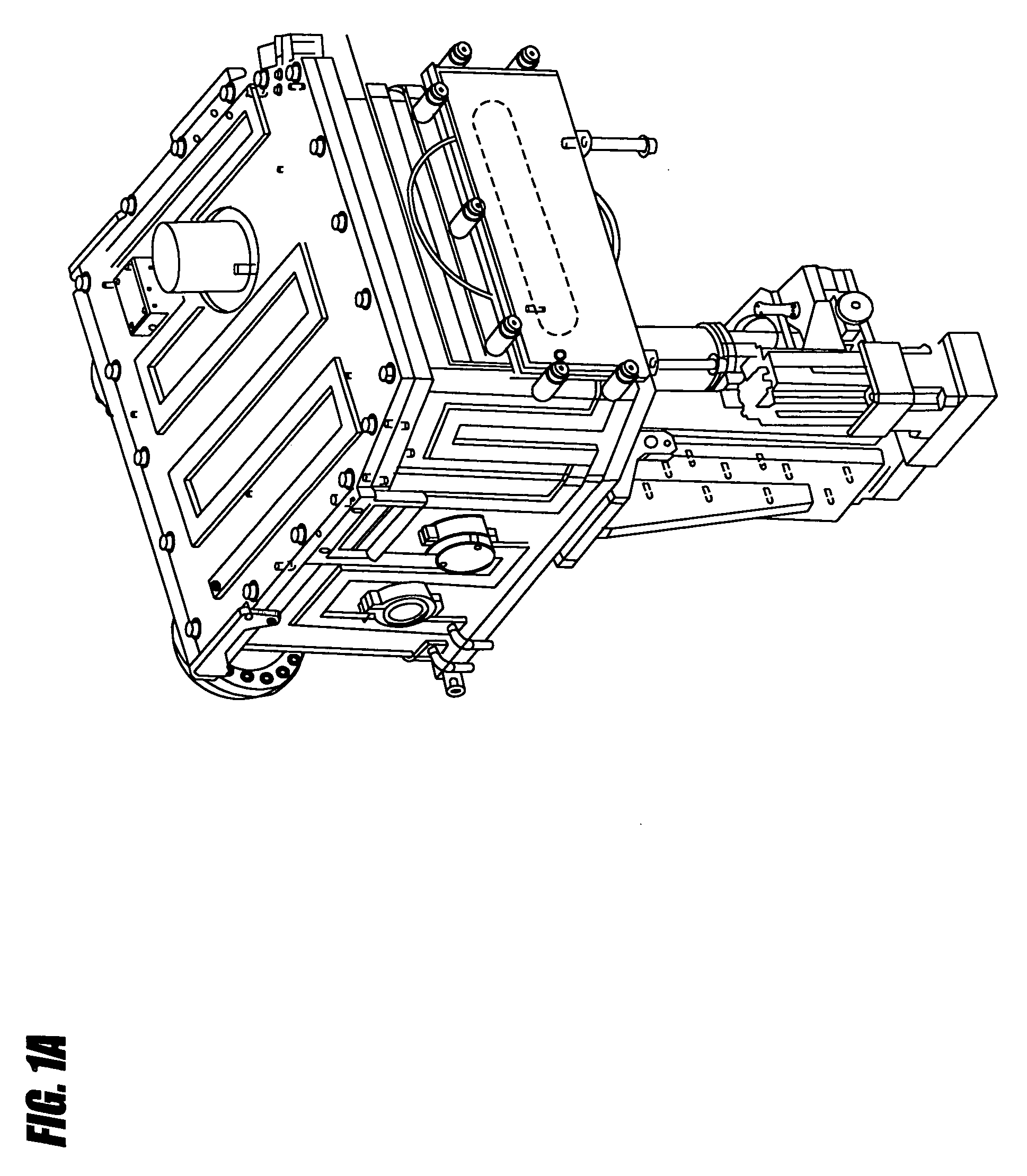
[0032]FIG. 1A is a perspective view of an embodiment of an ALD device 100. The ALD device 100 comprises a top member 110, a bottom member 112, and a front member 118, which together form a portion of a housing for the ALD device 100. In the embodiment illustrated in FIG. 1A, an upper heater 114 extends through the top member 110. The upper heater 114 is configured to maintain the temperature in the upper portion of the ALD device 100. Similarly, a lower heater 116 extends through the bottom member 112. The lower heater is configured to maintain the temperature in the lower portion of the ALD device 100.

[0033] The front member 118, which serves as a gate valve, of the ALD device 100 covers an opening 120. A dashed line outlines the opening 120 in FIG. 1A. Once the front member 118 is removed, the opening 120 can receive a wafer to be processed by the ALD device 100. In this way, the received wafer is placed in a deposition chamber within the ALD device 100. Once processing is comple...


PUM

PropertyMeasurementUnit
Fractionaaaaaaaaaa
Fractionaaaaaaaaaa
Thicknessaaaaaaaaaa

Abstract

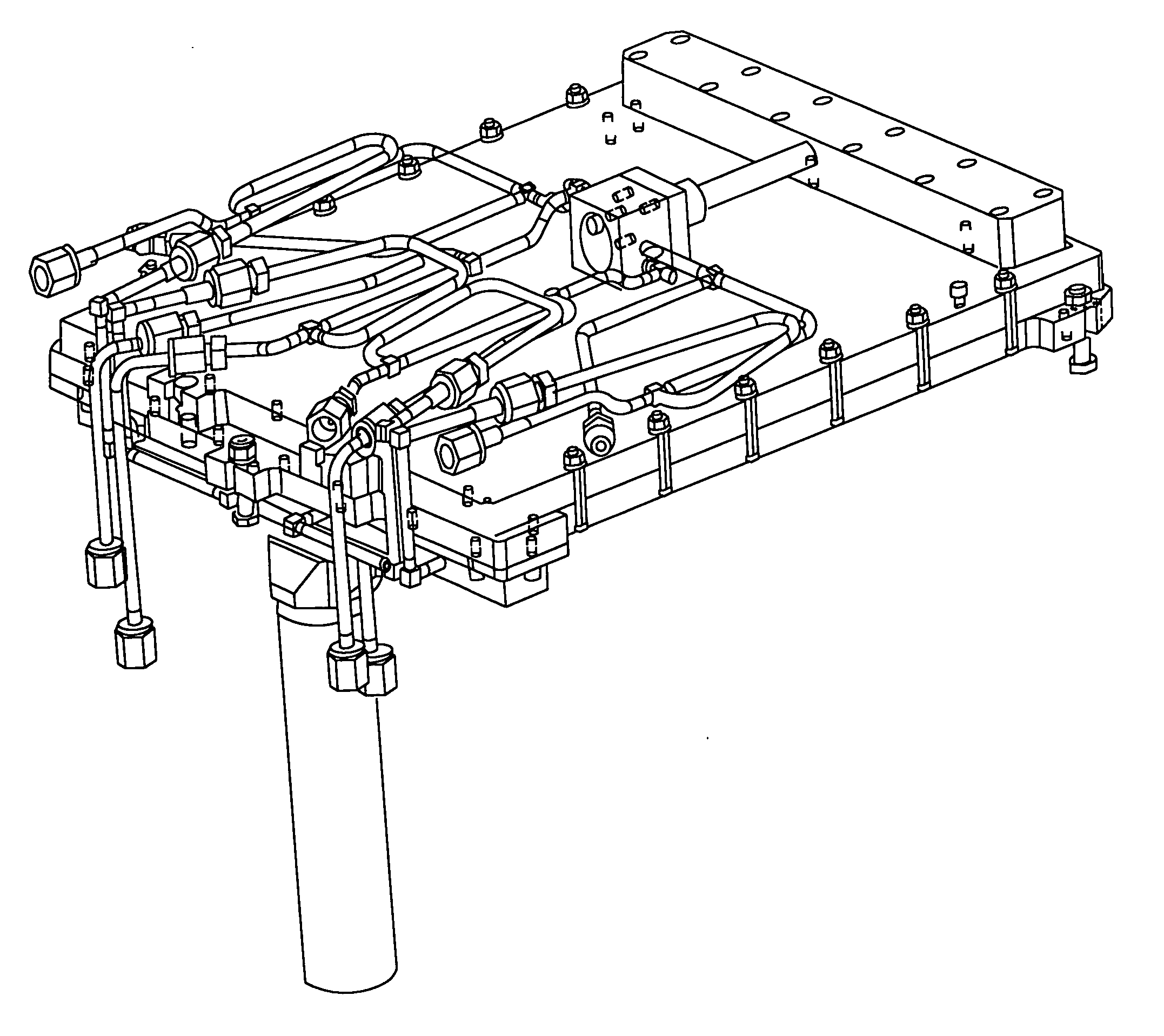
An atomic deposition (ALD) thin film deposition apparatus includes a deposition chamber configured to deposit a thin film on a wafer mounted within a space defined therein. The deposition chamber comprises a gas inlet that is in communication with the space. A gas system is configured to deliver gas to the gas inlet of the deposition chamber. At least a portion of the gas system is positioned above the deposition chamber. The gas system includes a mixer configured to mix a plurality of gas streams. A transfer member is in fluid communication with the mixer and the gas inlet. The transfer member comprising a pair of horizontally divergent walls configured to spread the gas in a horizontal direction before entering the gas inlet.

Description

RELATED APPLICATIONS [0001] This application claims the priority benefit under 35 U.S.C. § 119(e) of Provisional Application No. 60 / 645,581, filed on Jan. 18, 2005 and Provisional Application No. 60 / 656,832, filed Feb. 24, 2005, the entire contents of these applications are hereby incorporated herein by reference in their entiretyBACKGROUND OF THE INVENTION [0002] The present invention relates to equipment for chemical processes. In particular, the present invention relates to equipment for growing a thin film in a reaction chamber. Description of the Related Art [0003] There are several vapor deposition methods for depositing thin films on the surface of substrates. These methods include vacuum evaporation deposition, Molecular Beam Epitaxy (MBE), different variants of Chemical Vapor Deposition (CVD) (including low-pressure and organometallic CVD and plasma-enhanced CVD), and Atomic Layer Epitaxy (ALE), which is more recently referred to as Atomic Layer Deposition (ALD). [0004] ALD...

Claims


Application Information

Patent Timeline
IPC IPC(8): C23C16/00
CPCC23C16/4408C23C16/45525C23C16/45544C23C16/45563H01L21/68742C23C16/4586C30B35/00H01L21/67236H01L21/68714C23C16/45582C23C16/455C30B25/14C23C16/45517C23C16/45561C23C16/45587C23C16/45591C23C16/458C23C16/4582C23C16/4583H01L21/68785
Inventor VERGHESE, MOHITHFONDURULIA, KYLEWHITE, CARLSHERO, ERICBABIC, DARKOTERHORST, HERBERTPEUSSA, MARKOYAN, MIN
Owner ASM IP HLDG BV
Learn More