Shift register and display device having the same, and method thereof

a shift register and display device technology, applied in the field of shift registers and display devices, can solve the problems of deteriorating image display quality, decreasing the resolution of lcd devices, and increasing the deterioration of thin film transistors, so as to improve the driving margin of shift registers, the charging rate of capacitors, and the channel length of driving transistors of each stage.

Inactive Publication Date: 2006-11-30
SAMSUNG ELECTRONICS CO LTD
View PDF0 Cites 47 Cited by
  • Summary
  • Abstract
  • Description
  • Claims
  • Application Information

AI Technical Summary

Benefits of technology

[0020] According to the present invention, the output signals of the shift register are divided into a plurality of groups, and sequentially applied to the gate lines (e.g., the output signals are applied to the gate lines in sequence), so that the driving margin of the shift register is improved.
[0021] In addition, the channel length of the driving transistor of each of the stages of each of the gate driving parts is increased, as the number of each of the stages of each of the gate driving parts is increased. Therefore, the maximum current that can be applied to the driving transistor and the charging rate of the capacitor of each of the stages are increased, thus improving the waveform of the output signal.
[0022] Furthermore, the channel length of the carry transistor of each of the stages of each of the gate driving parts is increased, as the number of each of the stages of each of the gate driving parts is increased. Therefore, the maximum current that can be applied to the carry transistor is increased, thus improving the waveform of the carry signal.
[0023] Also, the width of the carry line of each of the stages of each of the gate driving parts is increased, as the number of each of the stages of each of the gate driving parts is increased. Therefore, the maximum current that can be applied to the carry line is increased, thus improving the waveform of the carry signal.
[0024] In addition, the current needed for driving the shift register may be decreased so that the shift register may be more highly integrated.

Problems solved by technology

Decreasing the channel length of each of the thin film transistors results in an increase in the deterioration of the thin film transistors and a decrease in the resolution of the LCD device.
In addition, the gate signal is delayed in the LCD panel, thus deteriorating image display quality.

Method used


Image

  • Shift register and display device having the same, and method thereof
  • Shift register and display device having the same, and method thereof
  • Shift register and display device having the same, and method thereof

Examples


Embodiment Construction

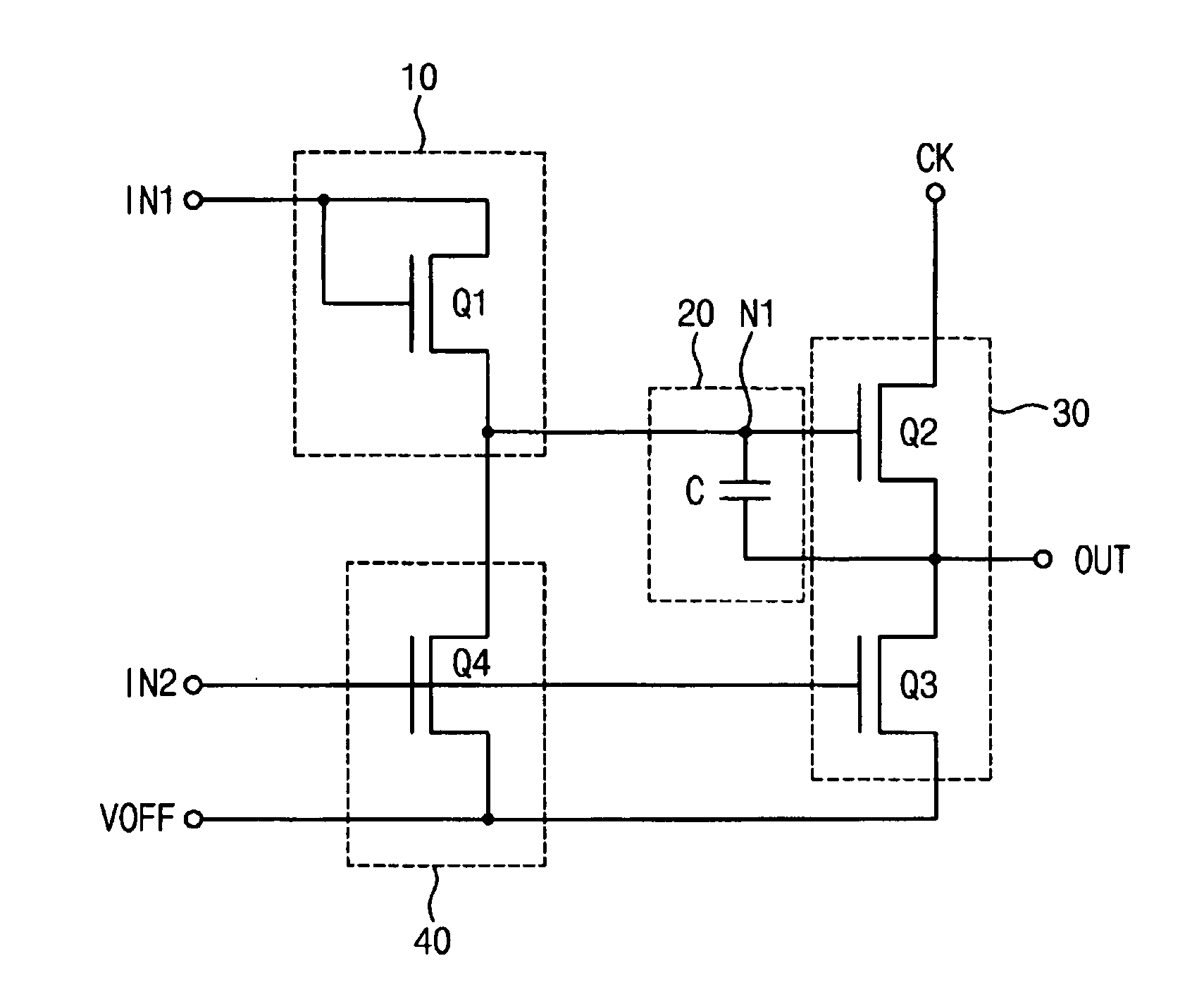
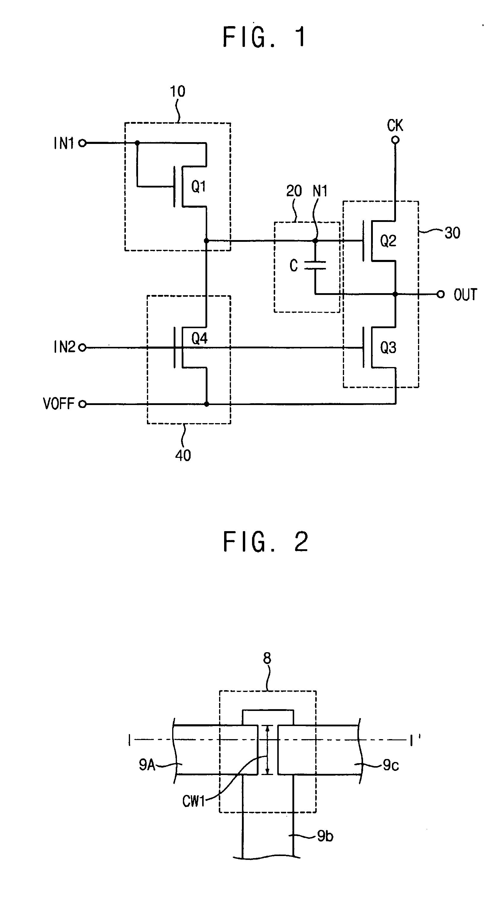
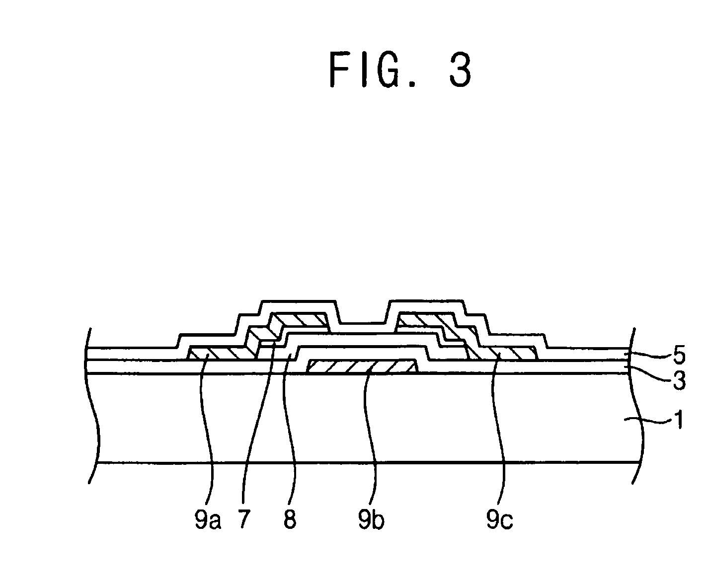
[0042] The invention is described more fully hereinafter with reference to the accompanying drawings, in which embodiments of the invention are shown. This invention may, however, be embodied in many different forms and should not be construed as limited to the embodiments set forth herein. Rather, these embodiments are provided so that this disclosure will be thorough and complete, and will fully convey the scope of the invention to those skilled in the art. In the drawings, the size and relative sizes of layers and regions may be exaggerated for clarity.

[0043] It will be understood that when an element or layer is referred to as being “on”, “connected to” or “coupled to” another element or layer, it can be directly on, connected or coupled to the other element or layer or intervening elements or layers may be present. In contrast, when an element is referred to as being “directly on,”“directly connected to” or “directly coupled to” another element or layer, there are no interveni...


PUM


Abstract

A shift register invention includes a plurality of stages outputting a plurality of output signals, in sequence. Each of the stages includes a driving part and a discharging part. The driving part includes a driving transistor. The driving transistor has a control electrode, a first electrode, a second electrode and a channel layer. The control electrode receives one of a start signal or an output signal of a previous stage. The first electrode receives a clock signal. The second electrode outputs an output signal of a present stage. The channel layer has a different length from a channel layer of a driving transistor of the previous stage. The discharging part discharges the output signal of the present stage based on an output signal of a next stage, therefore improving the electrical characteristics of the shift register.

Description

[0001] The present application claims priority to Korean Patent Application No. 2005-45566, filed on May 30, 2005, and all the benefits accruing therefrom under 35 U.S.C. §119, and the contents of which in its entirety are herein incorporated by reference. BACKGROUND OF THE INVENTION [0002] 1. Field of the Invention [0003] The present invention relates to a shift register, a display device having the shift register and a method of outputting signals in the shift register. More particularly, the present invention relates to a shift register having improved electrical characteristics, a display device having the shift register and a method of outputting signals in the shift register. [0004] 2. Description of the Related Art [0005] A flat panel display device includes a liquid crystal display (“LCD”) device, an organic light emitting display (“OLED”) device, or a plasma display (“PD”) panel device, for example. The flat panel display device has various characteristics such as thin thic...

Claims


Application Information

Patent Timeline
Patent Type & Authority Applications(United States)
IPC IPC(8): G09G3/36
CPCG09G3/3266G09G3/3275G09G3/3674G11C19/184G09G2300/0408G09G2310/06G09G3/3685G06F3/14G06F7/00
Inventor LEE, JONG-HWANLIM, DO-GILEE, KYE-HUN
Owner SAMSUNG ELECTRONICS CO LTD
Why Eureka
Try Eureka