
Electronic circuit protection device

a technology for electronic circuits and protective devices, applied in the direction of printed circuit manufacturing, magnetic/electric field screening, cross-talk/noise/interference reduction, etc., can solve the problems of affecting the proper operation of the radio transceiver circuit, protecting certain components of such an elementary electronic circuit, and arranging metal covers directly at the level of elementary electronic circuits, etc., to achieve the effect of reducing the number of metal covers

Active Publication Date: 2006-12-07
STMICROELECTRONICS SRL
View PDF15 Cites 84 Cited by
  • Summary
  • Abstract
  • Description
  • Claims
  • Application Information

AI Technical Summary

Benefits of technology

[0010] One embodiment of the present invention protects a portion of an electronic circuit, comprising at least one integrated circuit, against electromagnetic disturbances transmitted by another portion, comprising at least another integrated circuit, of the same electronic circuit and against electromagnetic disturbances originating from other electronic circuits.

Problems solved by technology

In particular, the proper operation of the radio transceiver circuit may be disturbed by the electromagnetic disturbances transmitted by the power amplifier circuit and other external circuits.
A difficulty then is to protect certain components of such an elementary electronic circuit against electromagnetic disturbances transmitted by other components of the same elementary electronic circuit.
Indeed, the arranging of metal covers directly at the level of the elementary electronic circuit is generally incompatible with conventional methods for manufacturing such circuits.

Method used


Image

  • Electronic circuit protection device
  • Electronic circuit protection device
  • Electronic circuit protection device

Examples


Embodiment Construction

[0035] For clarity, same elements have been designated with same reference numerals in the different drawings and, further, as usual in the representation of integrated circuits, the various drawings are not to scale.

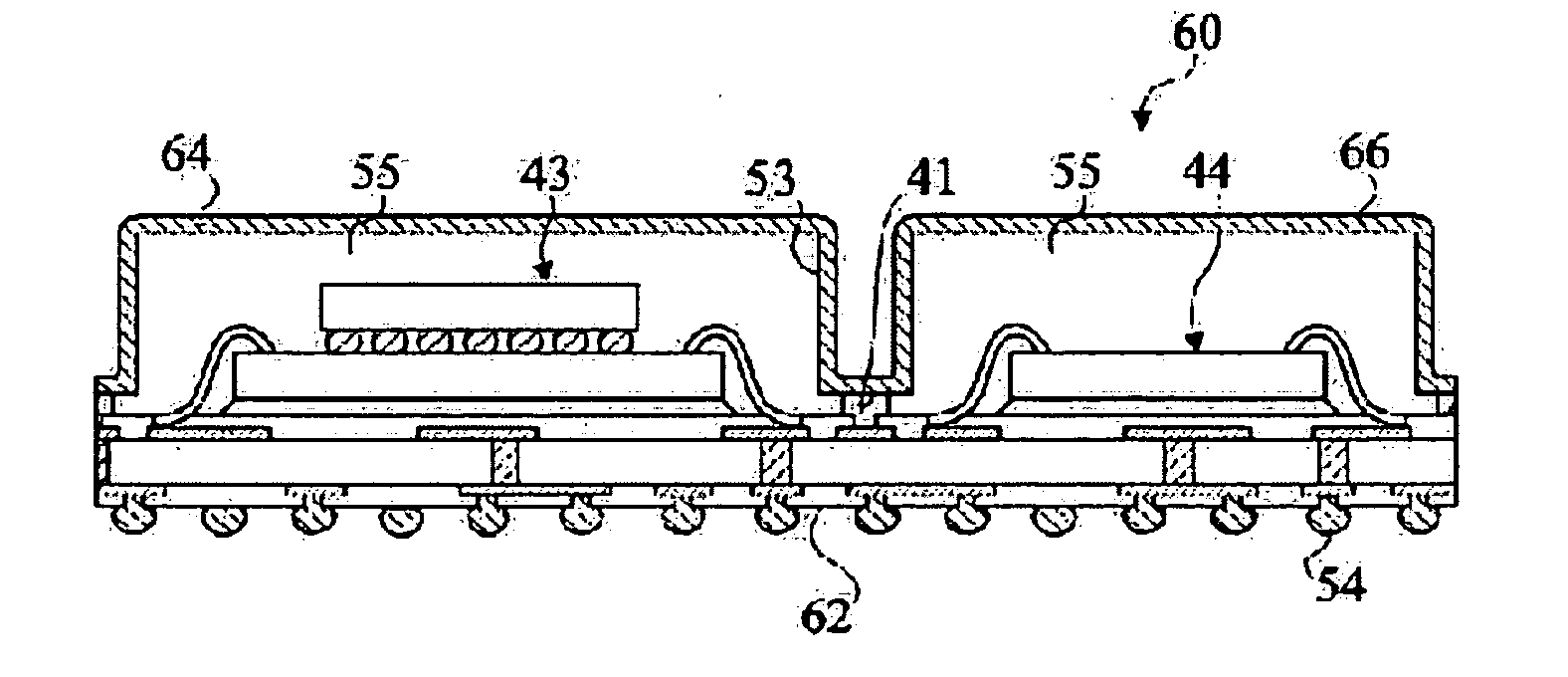
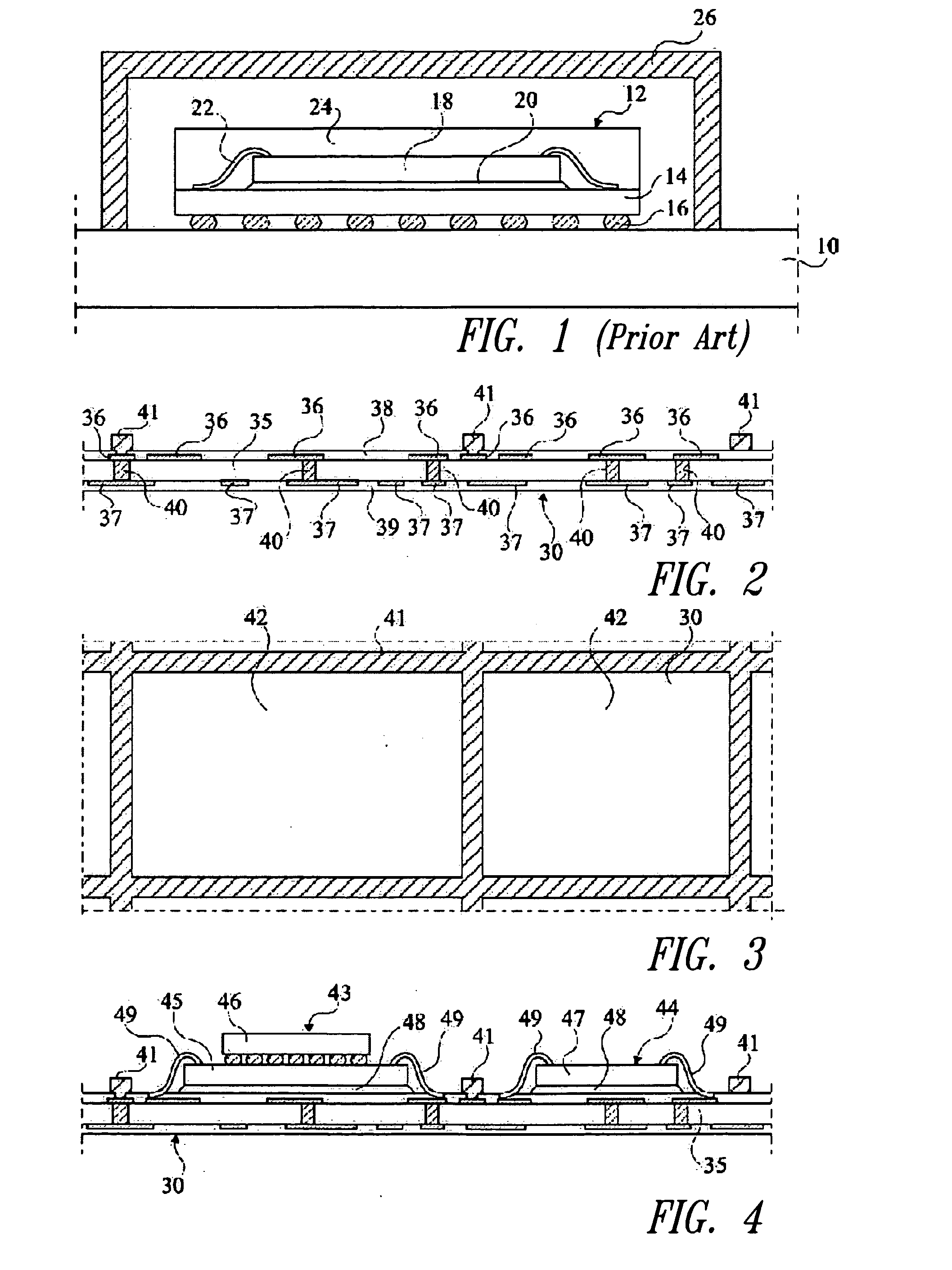
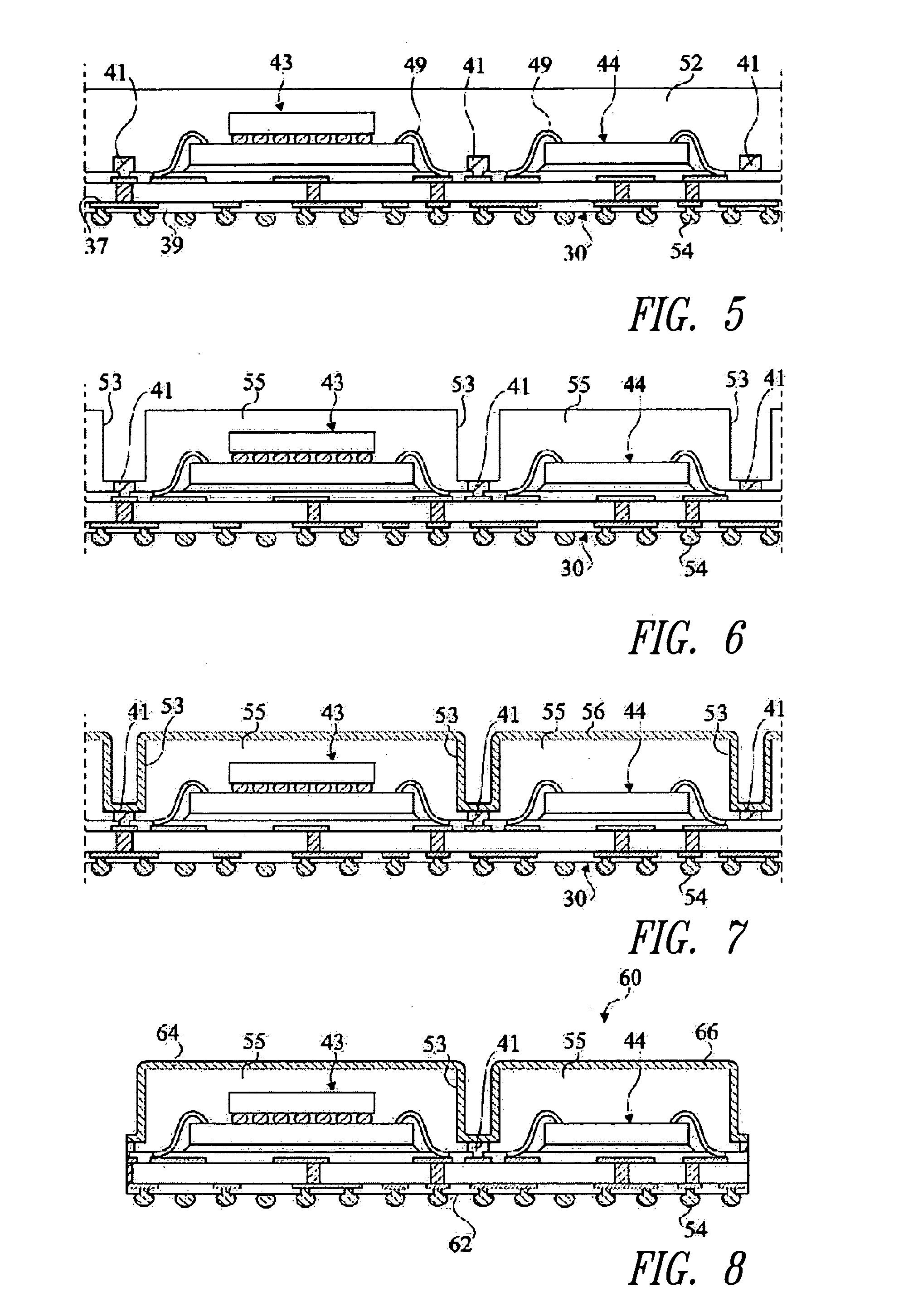
[0036] FIGS. 2 to 8 illustrate successive steps of a first example of embodiment of a method according to the present invention for manufacturing an electronic circuit protected against disturbances.

[0037]FIG. 2 is a cross-section view of a support 30 from which Ball Grid Array (BGA) packages on which electronic circuits will be formed must be obtained. At such a step of the manufacturing method, support 30 has the shape of a wafer formed of a central layer 35 made of an insulating material. Metal tracks 36, 37 are arranged on each surface of central layer 35 and are covered with an insulating layer 38, 39. Metal vias 40 are formed in central layer 35, each via 40 connecting a metal track 36 arranged on a surface of central layer 35 with a metal track 37 arranged on t...


PUM

PropertyMeasurementUnit
widthaaaaaaaaaa
widthaaaaaaaaaa
thicknessaaaaaaaaaa

Abstract

An electronic device protected against electromagnetic disturbances comprising: a support structure having a first and second electronic component, wherein the support structure includes a conductive means surrounding each of the first and second electronic components; a first and second insulating block formed overlying the first and second electronic components on the support structure; and a metal layer overlying the first and second insulating blocks that are formed over the first and second electronic components, wherein the metal layer is electrically connected to the support structure through the conductive means to protect the first and second electronic components from the electromagnetic disturbances irradiating from each of the first and second electronic components.

Description

BACKGROUND OF THE INVENTION [0001] 1. Field of the Invention [0002] The present invention relates to a device for protecting an electronic circuit and a method for forming such a device. [0003] 2. Description of the Related Art [0004] Many electronic circuits, for example for cell phones, are formed by attaching to a main support, generally called a motherboard, elementary electronic circuits formed separately, each fulfilling a specific function. As an example, for a cell phone, an elementary electronic circuit corresponds to a radio transceiver circuit, to be connected to the cell phone antenna, which demodulates the signals received at the antenna level and modulates the signals to be transmitted. Another elementary electronic circuit corresponds to a power amplifier circuit for amplifying the signals to be transmitted provided by the radio transceiver circuit. Each elementary electronic circuit is formed on a distinct support, for example, a ball grid array (BGA) or a land grid ...

Claims


Application Information

Patent Timeline
Patent Type & Authority Applications(United States)
IPC IPC(8): H05K9/00
CPCH01L21/561Y10T29/49126H01L23/49816H01L23/552H01L24/97H01L25/0655H01L25/18H01L2224/16145H01L2224/48091H01L2224/48227H01L2224/73265H01L2224/97H01L2924/01047H01L2924/01079H01L2924/14H01L2924/15311H01L2924/16152H01L2924/19041H01L2924/19043H05K1/0218H05K3/284H05K9/0022H01L23/3128Y10T29/49117Y10T29/49162H01L2924/1815H01L2924/01033H01L2924/01023H01L2924/01006H01L2924/01005H01L2224/73207H01L2224/32225H01L24/48H01L2224/85H01L2924/00014H01L2924/00012H01L2924/00H01L2924/181H01L24/73H01L2924/00011H01L2224/0401H01L2224/45099H01L2224/45015H01L2924/207
Inventor COFFY, ROMAIN
Owner STMICROELECTRONICS SRL
Features
  • Generate Ideas
  • Intellectual Property
  • Life Sciences
  • Materials
  • Tech Scout
  • Unparalleled Data Quality
  • Higher Quality Content
  • 60% Fewer Hallucinations
Learn More