Method and device for flattening surface of solid
a technology of flattening surface and solid surface, which is applied in the direction of electrical discharge tubes, decorative arts, electrical equipment, etc., can solve the problems of difficult to irradiate a gas cluster ion beam nearly perpendicularly, the problem of not being able to smooth the side wall surface, and the use of gas cluster ion beams for concave portions. , to achieve the effect of small surface roughness
- Summary
- Abstract
- Description
- Claims
- Application Information
AI Technical Summary
Benefits of technology
Problems solved by technology
Method used
Image
Examples
first embodiment
[First Embodiment]
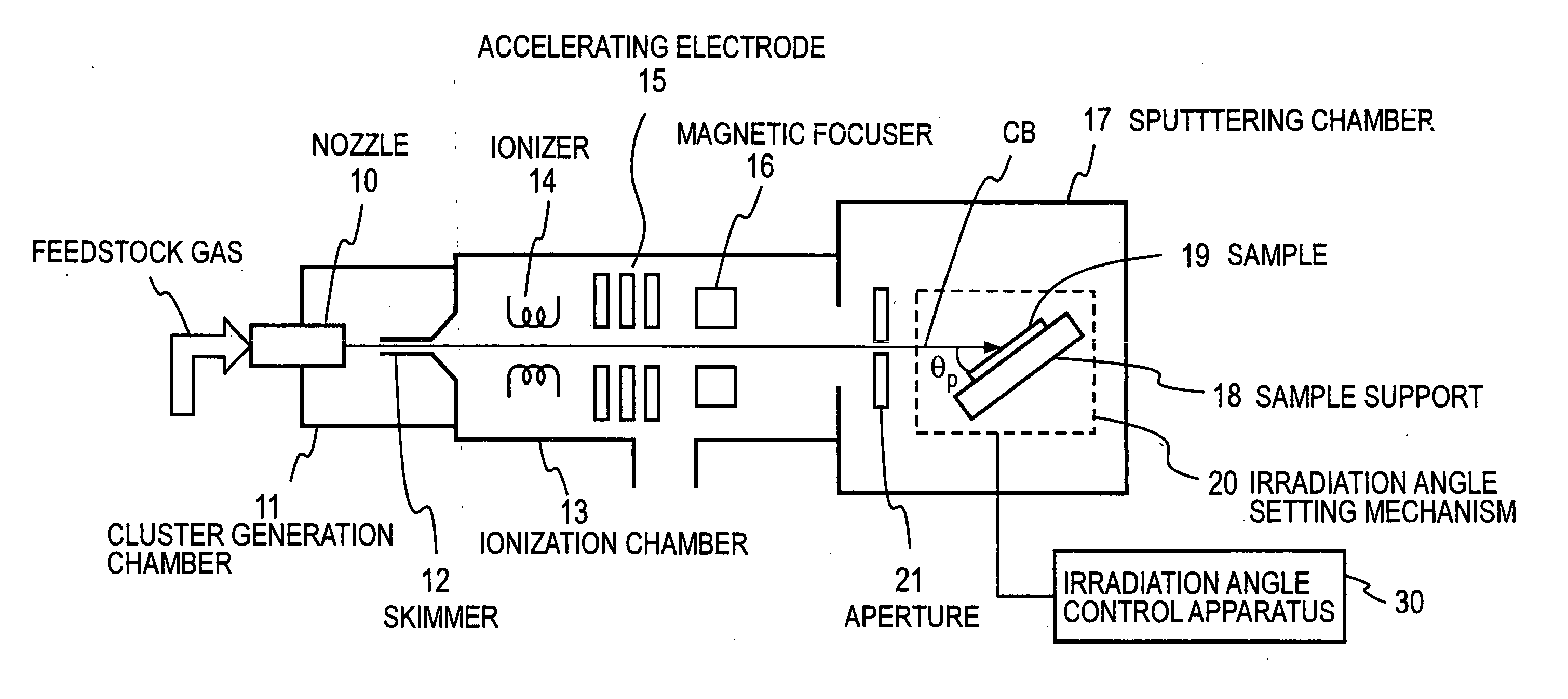
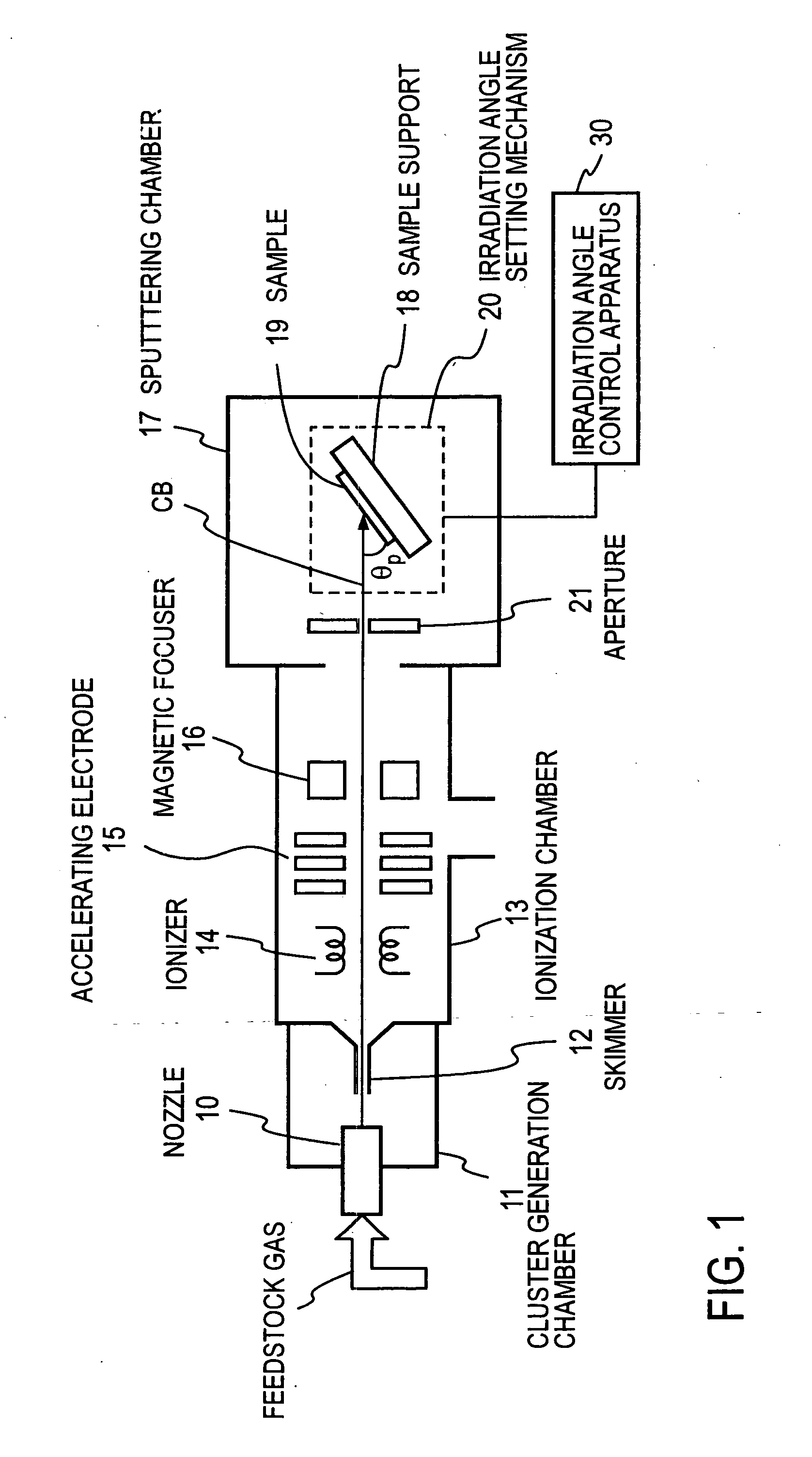
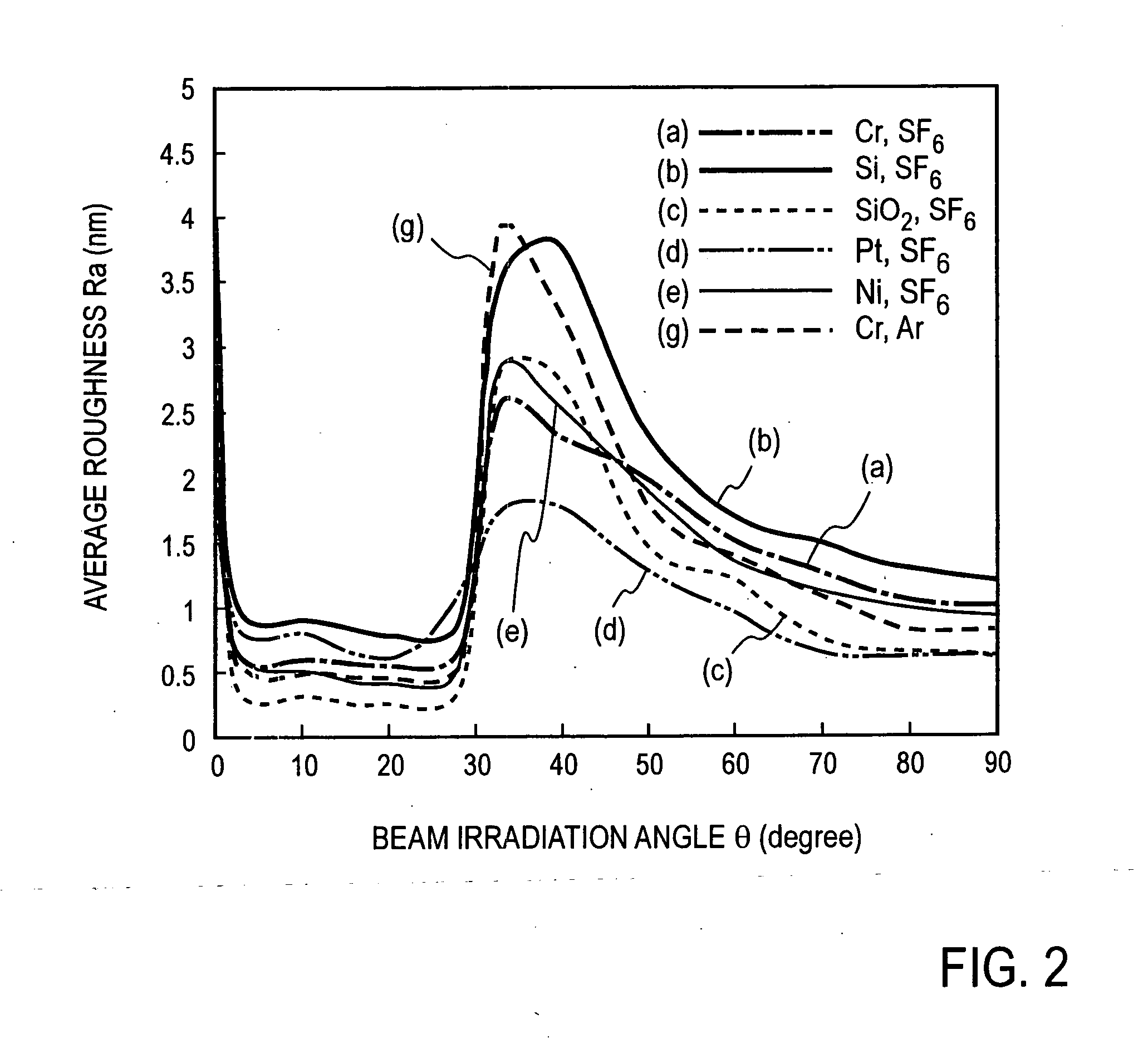
[0037] Using a mixture of SF6 gas and He gas as the feedstock gas, an SF6 cluster ion beam was generated with a size distribution having a peak for clusters aggregating approximately 500 SF6 molecules, and the SF6 cluster ions were accelerated by 30 kV and irradiated onto sample 19 at various irradiation angles θp with the irradiation dose set to 4×10¹⁵ ions / cm2. The surface roughness of a sample film was measured before and after irradiation with an Atomic Force Microscope (AFM). The measured results are shown in FIG. 2. As samples, the following films, deposited on a silicon substrate by a sputtering method, were respectively used: a chromium film (curve (a)), a platinum film (curve (d)), a nickel film (curve (e)), a silicon dioxide film (curve (c)), and a silicon film (curve (b)). For an irradiation angle range of 35°to 90°, the same trend is shown as that shown in Non-Patent Reference 2, namely that the average surface roughness Ra in this range is the smallest...
second embodiment
[Second Embodiment]
[0039] With the same conditions as in Embodiment 1 apart from setting the irradiation dose to 5×10¹⁴ ions / cm2, a Cr film was irradiated with SF6 cluster ions at an irradiation angle of 25°. The surface roughness of the Cr film after irradiation was measured using an atomic force microscope. The surface roughness Ra measured was 0.92 nm. Since the surface roughness of the Cr film for the case of an irradiation angle of 25° in FIG. 2 and a dose of 4×10¹⁵ ions / cm2 was approximately 0.5 nm, surface roughness is reduced when the irradiation dose is increased.
third embodiment
[Third Embodiment]
[0040] With the same apparatus as in Embodiment 1, but using Ar instead of SF6 as the feedstock gas, an Ar cluster ion beam was generated with a size distribution having a peak for clusters aggregating approximately 2000 Ar atoms, and the Ar cluster ions were accelerated by 30 kV and irradiated at various irradiation angles θp on a Cr film. The irradiation dose was set to 4×10¹⁵ ions / cm2. The surface roughness of the Cr film was measured before and after irradiation with an Atomic Force Microscope (AFM). The measured results are shown in curve (g) of FIG. 2. Also, the Cr film is a film formed by sputtering on a silicon substrate.
PUM
| Property | Measurement | Unit |
|---|---|---|
| angle | aaaaa | aaaaa |
| irradiation angle | aaaaa | aaaaa |
| angle | aaaaa | aaaaa |
Abstract
Description
Claims
Application Information


