Integrated circuits with inductors in multiple conductive layers

a technology of inductors and conductive layers, applied in the direction of transformers/inductance details, printed inductances, semiconductor/solid-state device details, etc., can solve the problems of unsymmetrical location within the inductor, differential inductor design does not achieve perfect symmetry, etc., to achieve asymmetrical symmetry of two inductors, increase inductance, and minimize the effect of asymmetry

Active Publication Date: 2006-12-21
INFINEON TECH AG
View PDF7 Cites 125 Cited by
  • Summary
  • Abstract
  • Description
  • Claims
  • Application Information

AI Technical Summary

Benefits of technology

[0014] Advantages of preferred embodiments of the present invention include providing pairs of coupled inductors wherein the two inductors have very symmetric inductance, resistance, and capacitance values. Differential inductors with increased inductance may be achieved by utilizing a greater number of conductive layers of integrated circuits, and by increasing the number of windings of the portions of the inductors within one or more conductive layers. Asymmetry of the two inductors is minimized by via positioning, using appropriate layouts, and by the use of notches at the end of the inductor portions for accommodating the via positioning to achieve increased symmetry.

Problems solved by technology

However, this differential inductor design does not achieve perfect symmetry, because the connection structure that is used to connect the partial inductors introduces an asymmetry.
However, the location within the inductor is unsymmetrical, e.g., one half inductor has its underpasses nearer to the middle pin or center tap, and the other one nearer to the A or B voltage input.

Method used


Image

  • Integrated circuits with inductors in multiple conductive layers
  • Integrated circuits with inductors in multiple conductive layers
  • Integrated circuits with inductors in multiple conductive layers

Examples


Embodiment Construction

[0040] The making and using of the presently preferred embodiments are discussed in detail below. It should be appreciated, however, that the present invention provides many applicable inventive concepts that can be embodied in a wide variety of specific contexts. The specific embodiments discussed are merely illustrative of specific ways to make and use the invention, and do not limit the scope of the invention.

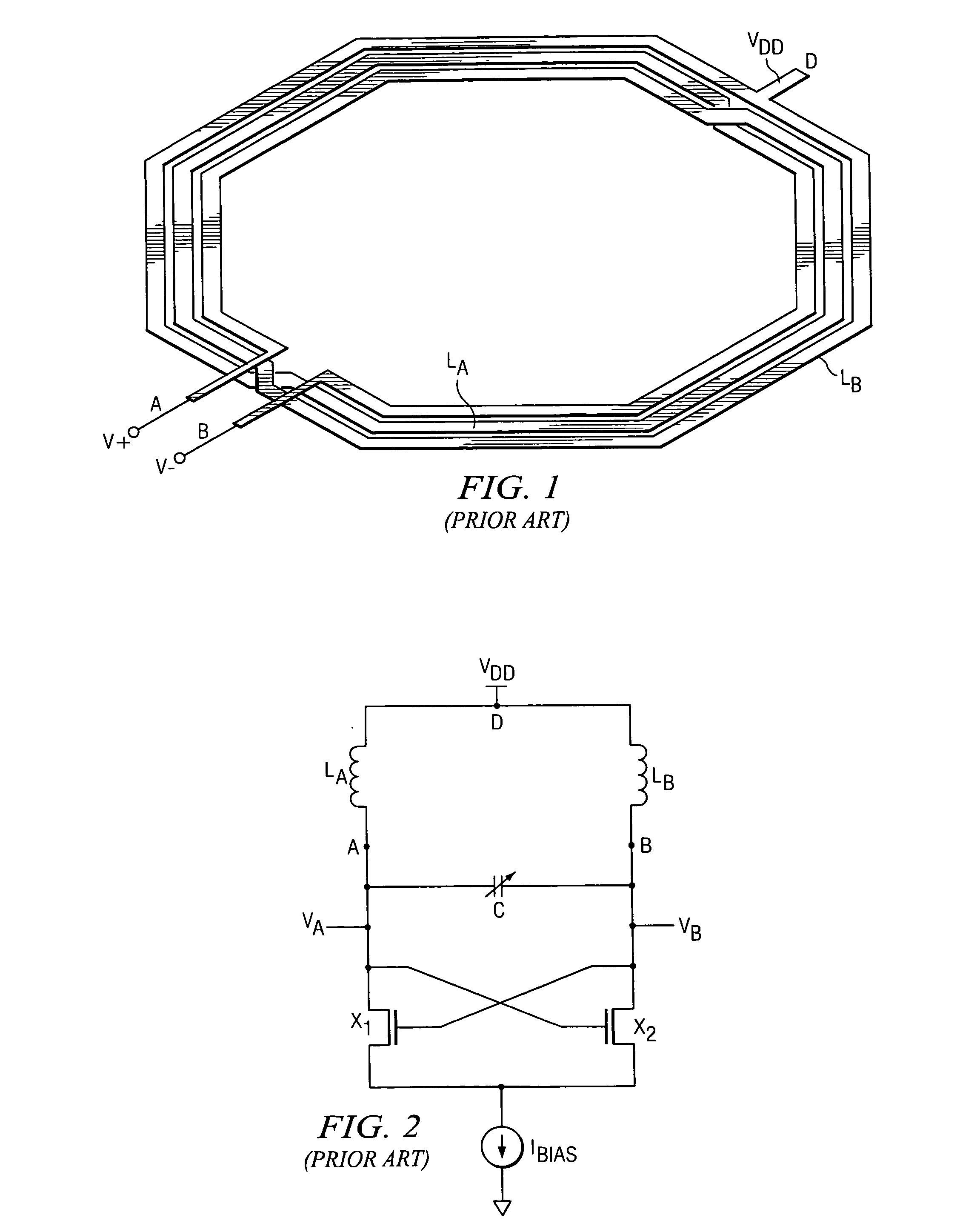
[0041] The present invention will be described with respect to preferred embodiments in a specific context, namely differential inductors used in a VCO circuit. Embodiments of the invention may also be applied, however, to other RF designs requiring the use of inductors, for example, such as transformers and other circuits or circuit components requiring two coupled inductors.

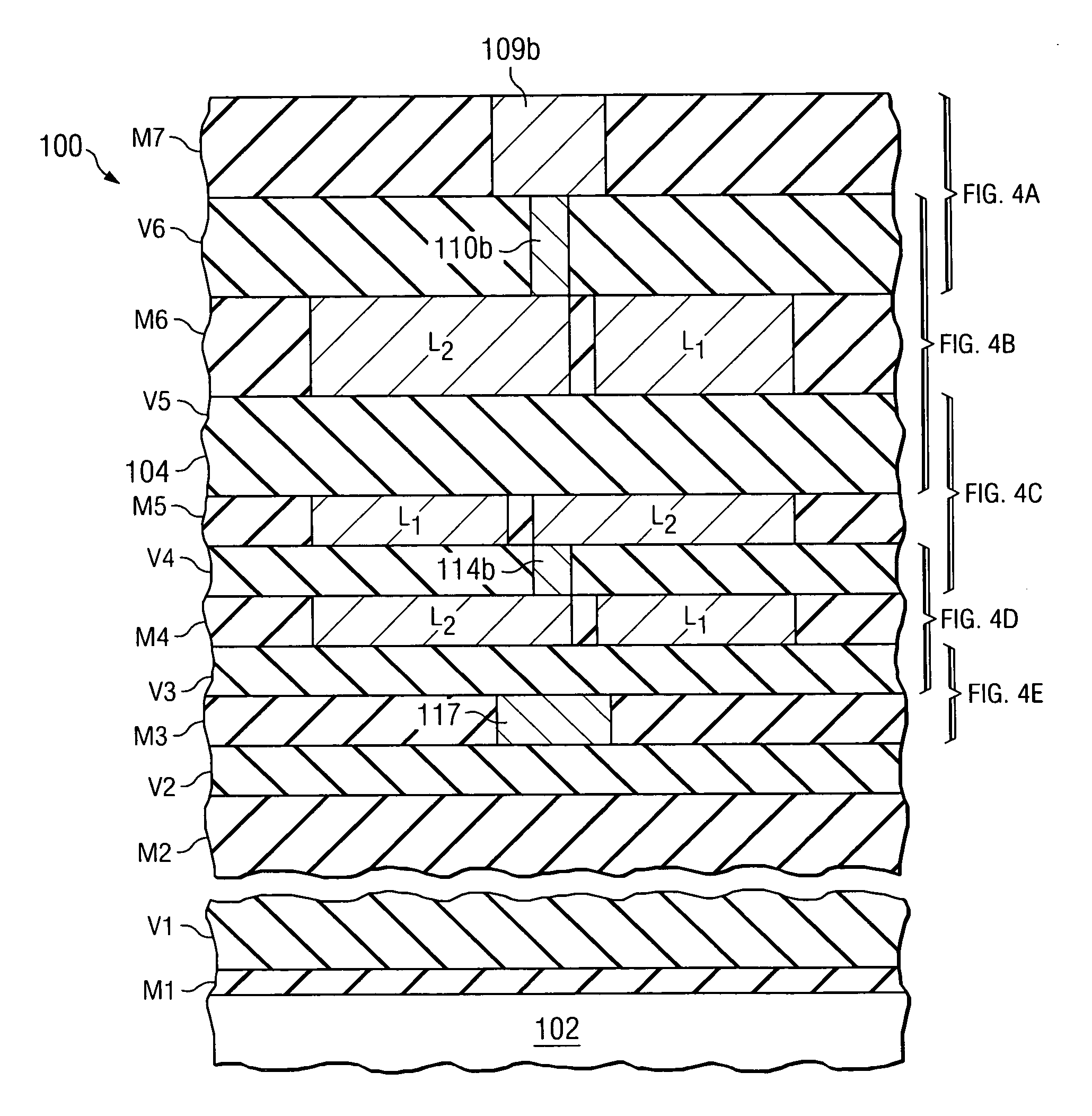
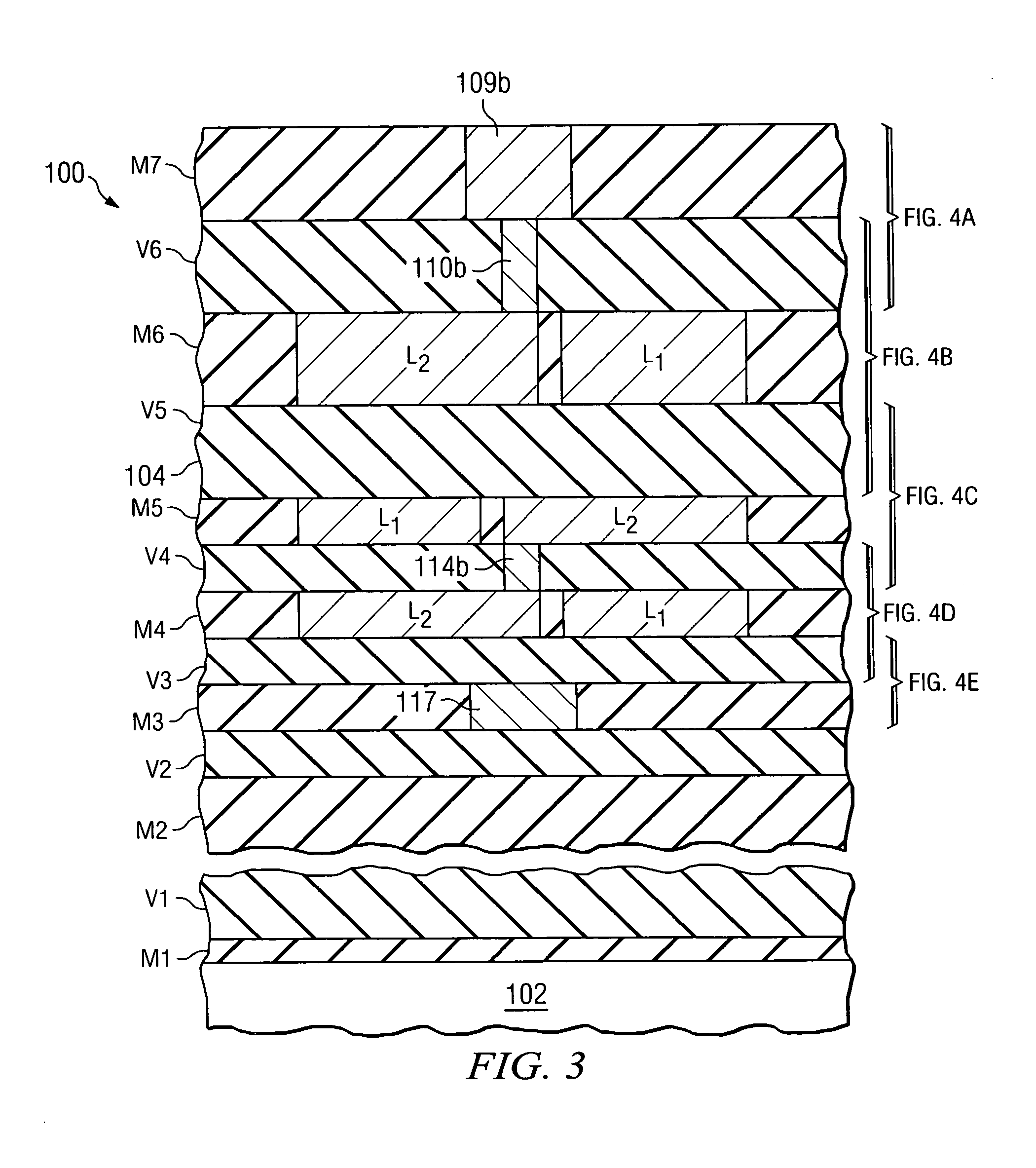
[0042]FIG. 3 is a cross-sectional view of an embodiment of the present invention, wherein a semiconductor device 100 includes a differential inductor formed in multiple conductive layers M1, M2, M3, M...


PUM

PropertyMeasurementUnit
cross-sectional areasaaaaaaaaaa
cross-sectional areaaaaaaaaaaa
forceaaaaaaaaaa

Abstract

Two inductors formed in multiple layers of conductive layers of integrated circuits are disclosed. Symmetric portions of a first inductor and a second inductor are formed in two or more conductive layers. Portions of the first inductor in adjacent conductive layers are connected by vias, and portions of the second inductor in adjacent conductive layers are connected by vias. The first and second inductor portions form a substantially loop-shaped structure in each conductive layer. The first and second inductor vias may be positioned at the same position within the substantially loop-shaped inductor structure by alternating inner and outer radiuses, or the vias for the second inductor may be positioned opposite the vias for the first inductor within the substantially loop-shaped inductor structure, using notches in the first and second inductor portions.

Description

TECHNICAL FIELD [0001] The present invention relates generally to radio frequency (RF) integrated circuits (IC's), and more particularly to structures for inductors and methods of manufacturing thereof. BACKGROUND [0002] An inductor in electronics applications typically comprises a coil of wire that exhibits electromagnetic properties when current is run through the coil of wire. In general, an inductor can store energy in its magnetic field, and an inductor tends to resist a change in the amount of current flowing through it, for example. The inductance of an inductor is dependent upon several factors. One factor is the number of windings: the larger the number of windings, the higher the inductance. Another factor is the cross-sectional area of the coil: more area results in higher inductance. Another factor is the width of windings: a larger width results in a higher ratio of outer to inner diameter of the coil and reduced inductance. These factors also affect the parasitic capac...

Claims


Application Information

Patent Timeline
Patent Type & Authority Applications(United States)
IPC IPC(8): H01F27/28
CPCH01F2021/125H01F17/0006H01L23/5227
Inventor BAUMGARTNER, PETERBENETIK, THOMAS
Owner INFINEON TECH AG
Why Eureka
Try Eureka