Optical stacked structure inspecting method and optical stacked structure inspecting apparatus

Inactive Publication Date: 2006-12-21
RICOH KK
View PDF14 Cites 6 Cited by
  • Summary
  • Abstract
  • Description
  • Claims
  • Application Information

AI Technical Summary

Benefits of technology

[0013] Another and more specific object of the present invention is to provide an optical stacked structure inspecting methods, an optical stacked structure inspecting apparatus, an optical stacked structure producing method and an optical stacked structure producing apparatus, which enable simple inspection of the thickness of each layer of the optical stacked structure having a reflection layer and at least one light transmitting thin film stacked on a substrate.
[0014] Still another object of the present invention is to provide an optical stacked structure inspecting method for inspecting an optical stacked structure having a reflection layer and at least one light transmitting thin film sequentially stacked on a substrate, the optical stacked structure inspecting method comprising (a) irradiating inspection light on the optical stacked structure from a side provided with the light transmitting thin film; (b) measuring a light intensity of reflected light from each layer, that changes depending on a change in an optical path length to each layer; and (c) inspecting a thickness of the light transmitting thin film based on the light intensity of reflected light for a specific wavelength. According to the optical stacked structure inspecting method of the present invention, it is possible to enable simple inspection of the thickness of each layer of the optical stacked structure.
[0015] A further object of the present invention is to provide an optical stacked structure inspecting apparatus for inspecting an optical stacked structure having a reflection layer and at least one light transmitting thin film sequentially stacked on a substrate, the optical stacked structure inspecting apparatus comprising a light source configured to irradiate inspection light on the optical stacked structure from a side provided with the light transmitting thin film, and an inspecting part configured to measuring a light intensity of reflected light from each layer, that changes depending on a change in an optical path length to each layer, and to inspect a thickness of the light transmitting thin film based on the light intensity of reflected light for a specific wavelength. According to the optical stacked structure inspecting apparatus of the present invention, it is possible to enable simple inspection of the thickness of each layer of the optical stacked structure.

Problems solved by technology

However, when producing this type of optical recording medium by forming the recording layer and the semi-transparent reflection layer on each substrate and bonding the first and second substrates, there was a problem in that the thicknesses of the dye layer formed on the total reflection layer and the dielectric layer formed on the dye layer cannot be measured using the transmitted light because the light cannot be transmitted through the total reflection layer of the second substrate.

Method used


Image

  • Optical stacked structure inspecting method and optical stacked structure inspecting apparatus
  • Optical stacked structure inspecting method and optical stacked structure inspecting apparatus
  • Optical stacked structure inspecting method and optical stacked structure inspecting apparatus

Examples


first embodiment

Sample

[0052] A concavo-convex pattern of guide grooves having a depth of approximately 30 nm and a groove width of approximately 0.25 μm were formed with a track pitch of 0.74 μm on a polycarbonate substrate having a diameter of 120 mm and a thickness of 0.60 mm. a material having a composition Ag (98 wt %) / Cu (2 wt %) was sputtered to a thickness of approximately 140 nm by a sputtering apparatus (model name Big Sprinter) manufactured by Unaxis using Ar as a sputtering gas at a sputtering pressure of 6.0×10⁻³ Torr and a D.C. sputtering power of 3.5 kW, so as to form the reflection layer. Next, a squarylium dye compound was spin-coated on the reflection layer to a layer thickness such that the absorbance at the maximum absorption wavelength λmax becomes 1.02, 1.06, 1.12 and 1.16.

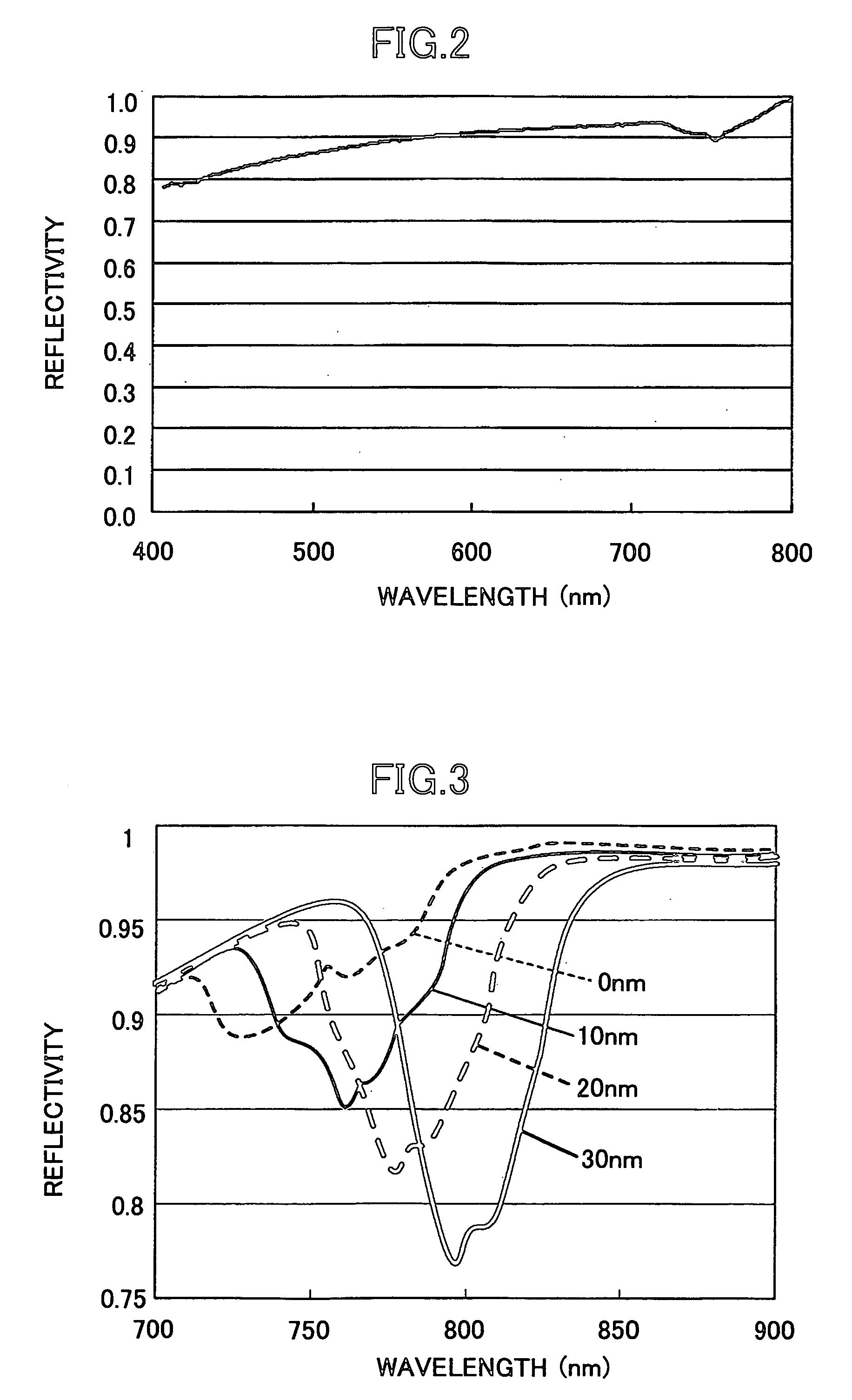
[0053] Thereafter, the dye surface reflectivity of the substrate structure of this first embodiment sample was measured by ETA-RT at the wavelength of 740 nm. The results shown in FIG. 10 were obtained by th...

second embodiment

Sample

[0054] A material having a composition ZnS (80 mol %) / SiO2 (20 mol %) was sputtered to thicknesses of 120 nm, 130 nm, 140 nm and 150 nm on the substrate structure of the first embodiment sample described above by the sputtering apparatus (model name Big Sprinter) manufactured by Unaxis using Ar as the sputtering gas at the sputtering pressure of 4.0×10⁻³ Torr and an RF sputtering power of 4.0 kW, so as to form the dielectric layer.

[0055] Then, the dielectric surface reflectivity of the substrate structure of this second embodiment sample was measured similarly by the ETA-RT at the wavelength of 500 nm. The results shown in FIG. 11 were obtained by this measurement. FIG. 11 is a diagram showing the relationship of the reflectivity for the wavelength of 500 nm and the dielectric layer thickness, and it may be seen that there is an extremely strong correlation between the two.

third embodiment

Sample

[0056] A concavo-convex pattern of guide grooves having a depth of approximately 30 nm and a groove width of approximately 0.25 μm were formed with a track pitch of 0.74 μm on a polycarbonate substrate having a diameter of 120 mm and a thickness of 0.60 mm. A material having a composition Ag (98 wt %) / Cu (2 wt %) was sputtered to a thickness of approximately 120 nm by the sputtering apparatus (model name Big Sprinter) manufactured by Unaxis using Ar as the sputtering gas at the sputtering pressure of 6.0×10⁻³ Torr and the D.C. sputtering power of 3.5 kW, so as to form the reflection layer. Next, a material having a composition ZnS (80 mol %) / SiO2 (20 mol %) was sputtered to thicknesses of 10 nm, 20 nm and 30 nm on the substrate structure by the sputtering apparatus (model name Big Sprinter) manufactured by Unaxis using Ar as the sputtering gas at the sputtering pressure of 4.0×10⁻³ Torr and the RF sputtering power of 4.0 kW, so as to form the dielectric layer.

[0057] Then, the...


PUM


Abstract

An inspecting method inspects an optical stacked structure having a reflection layer and at least one light transmitting thin film sequentially stacked on a substrate. The inspecting method irradiates inspection light on the optical stacked structure from a side provided with the light transmitting thin film, measures a light intensity of reflected light from each layer, that changes depending on a change in an optical path length to each layer, and inspects a thickness of the light transmitting thin film based on the light intensity of reflected light for a specific wavelength.

Description

BACKGROUND OF THE INVENTION [0001] 1. Field of the Invention [0002] The present invention generally relates to optical stacked structure inspecting methods and optical stacked structure inspecting apparatuses, and more particularly to an optical stacked structure inspecting method and an optical stacked structure inspecting apparatus for inspecting a dye layer thickness and / or a dielectric layer thickness of an optical stacked structure in which a reflection layer and an organic dye layer are successively stacked on a substrate or, a reflection layer, an organic dye layer and a dielectric layer are successively stacked on a substrate. The present invention also relates to a method and an apparatus for producing such an optical stacked structure. [0003] 2. Description of the Related Art [0004] Generally known write-once type optical recording media, to which information can be written once by a laser beam, include CD-R, DVD+R and DVD-R. Such write-once type optical recording media ha...

Claims


Application Information

Patent Timeline
IPC IPC(8): G01B11/02
CPCG01N21/9506G01B11/0625
Inventor NAKAMURA, YUKI
Owner RICOH KK
Why Eureka
Try Eureka