Integrated optical mode shape transformer and method of fabrication

a technology of optical mode and shape transformer, which is applied in the field of integrated optical mode shape transformer and fabrication method, can solve the problems of not being able to achieve the effect of lithographic process, not being able to achieve mode transformation to or from high index difference waveguide, and not being able to meet the requirements of etching techniques that are not well controlled and therefore difficult to manufactur

Active Publication Date: 2006-12-21
INFINERA CORP
View PDF13 Cites 72 Cited by
  • Summary
  • Abstract
  • Description
  • Claims
  • Application Information

AI Technical Summary

Problems solved by technology

Vertical tapering uses special etching techniques that are not well-controlled and therefore difficult to manufacture.
This is not a suitable method for mode transformation to or from a high index difference waveguide.
The taper is required to also come down to a sharp point, which makes it almost impossible to perform in a lithographic process.
The major drawback of this approach lies in the fact that the deconfinement of the mode is done entirely in the active guide.
This leads to a deterioration of the performance characteristics of the component, especially its threshold current and its efficiency.
Furthermore, the optical coupling losses with a single-mode optical fiber are still high.
None of the prior art provides for an efficient mode transformation between a low index difference and a high index difference waveguide on a microchip.

Method used


Image

  • Integrated optical mode shape transformer and method of fabrication
  • Integrated optical mode shape transformer and method of fabrication
  • Integrated optical mode shape transformer and method of fabrication

Examples


Embodiment Construction

[0035] The following description will further help to explain the inventive features of the Optical Mode Shape Transformer.

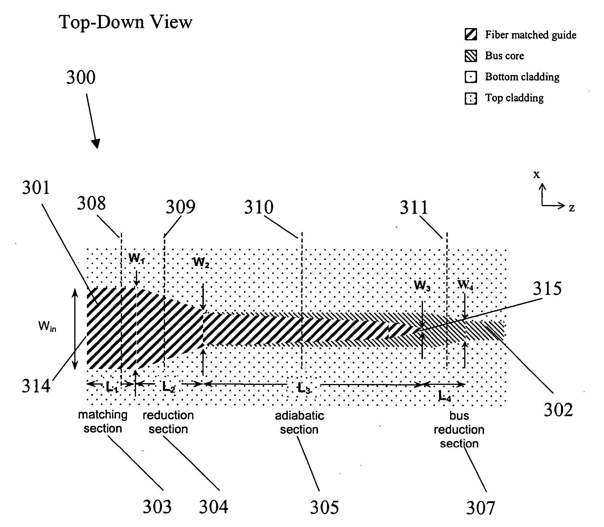
[0036] The approach used in this invention is to separate the problem into two steps with definitive objectives. The first objective is to get optical power from the SM fiber onto the chip with the highest possible efficiency. Once high efficiency connectivity and optical power transmission is established onto the chip, power is then transferred into the HC waveguide via an on chip mode transformer.

[0037]FIG. 3 shows a perspective view of the mode shape transformer. The mode transformer has two waveguide layers, one contiguously on top of the other. The first layer (302), also called the bottom layer, is the core of the HC waveguide layer that makes up the rest of chip's optical circuit. This waveguide is often called the “bus”. The second layer (301), which is on top of the first, is usually a much thicker layer and in conduction with the first layer, is used...


PUM


Abstract

An integrated optical mode transformer provides a low loss interconnection between an optical fiber and an integrated optic waveguide having a spot size different from that of the fiber. The mode transformer is comprised of two waveguide layers, an upper layer and a lower layer, with the upper layer being contiguous to the lower layer. The lower layer is the integrated optic waveguide layer forming the optical circuit. The input dimensions of the composite two-waveguide structure supports a fundamental mode that accepts all of the light present on the optical fiber. The upper waveguide layer is tapered down from an input width to an output width and then terminates in such a way that at the termination substantially all of the input optical power resides in the lower waveguide layer. The two-waveguide layer structure is fabricated by deposition and planarization techniques.

Description

CROSS-REFERENCE TO RELATED APPLICATIONS [0001] The present application is a continuation of U.S. Ser. No. 10 / 684,899, filed on Oct. 9, 2003, the entire content of which is hereby incorporated herein by reference.BACKGROUND OF THE INVENTION [0002] 1. Field of Invention [0003] This invention relates to a structure for the low loss connection of an optical fiber to an integrated optical waveguide having different dimensions from the fiber. More specifically it relates to a mode shape transformer fabricated as an integrated optical waveguide structure that is used for changing the shape and dimension of an optical mode field of an integrated optical waveguide so that it matches the mode field shape of an input optical fiber. [0004] 2. Background of the Invention [0005] The invention relates to the field of semiconductor and dielectric optical components used for optical transmission or optical digital data processing. It pertains especially to all optical components comprising active an...

Claims


Application Information

Patent Timeline
Patent Type & Authority Applications(United States)
IPC IPC(8): G02B6/26
CPCG02B6/305G02B6/1228
Inventor LITTLE, BRENT E.
Owner INFINERA CORP
Why Eureka
Try Eureka