Apparatus and method for removing semiconductor chip

a technology of apparatus and semiconductor chip, which is applied in the direction of metal sawing accessories, transportation and packaging, manufacturing tools, etc., can solve the problems of insufficient removal operation, and inability to thoroughly perform the removal operation, so as to prevent damage to the semiconductor chip and the like, and reduce the bonding force

Inactive Publication Date: 2006-12-21
PANASONIC CORP
View PDF9 Cites 8 Cited by
  • Summary
  • Abstract
  • Description
  • Claims
  • Application Information

AI Technical Summary

Benefits of technology

[0012] Accordingly, in order to solve the above problems, an object of the present invention is to provide an apparatus and method for removing semiconductor chip and an apparatus for feeding semiconductor chips without damaging thinner semiconductor chips in particular, in which one out of a plurality of semiconductor chips formed from a diced semiconductor wafer is removed from a pressure-sensitive adhesive sheet that holds the semiconductor chips by adhering thereto, so that the semiconductor chip is possible to be extracted from the adhesive sheet.
[0050] Further, the reciprocal movement of the removing member is achieved by vibrating the removing member, which makes it possible to simplify the structure of the removing member moving device.

Problems solved by technology

However, with development of the thinner IC chips, even if the adhesion of the IC chips to wafer sheets are decreased by the partial removal, the problem that the IC chips may be damaged by push-up operation still exists as long as the push-up operation by the push-up pin is performed.
Consequently, in this sucking and extracting operation, force to remove the IC chips from the wafer sheets is applied to the IC chips themselves, and the thinner IC chips in particular has a problem that the force inflicts damage thereon or if the force does not go so far as inflicting damage, then the removal operation may not be performed thoroughly.

Method used


Image

  • Apparatus and method for removing semiconductor chip
  • Apparatus and method for removing semiconductor chip
  • Apparatus and method for removing semiconductor chip

Examples


Embodiment Construction

[0061] Before the description of the present invention proceeds, it is to be noted that like parts are designated by like reference numerals throughout the accompanying drawings.

[0062] Hereinbelow, the embodiments of the present invention will be described in detail with reference to the accompanying drawings.

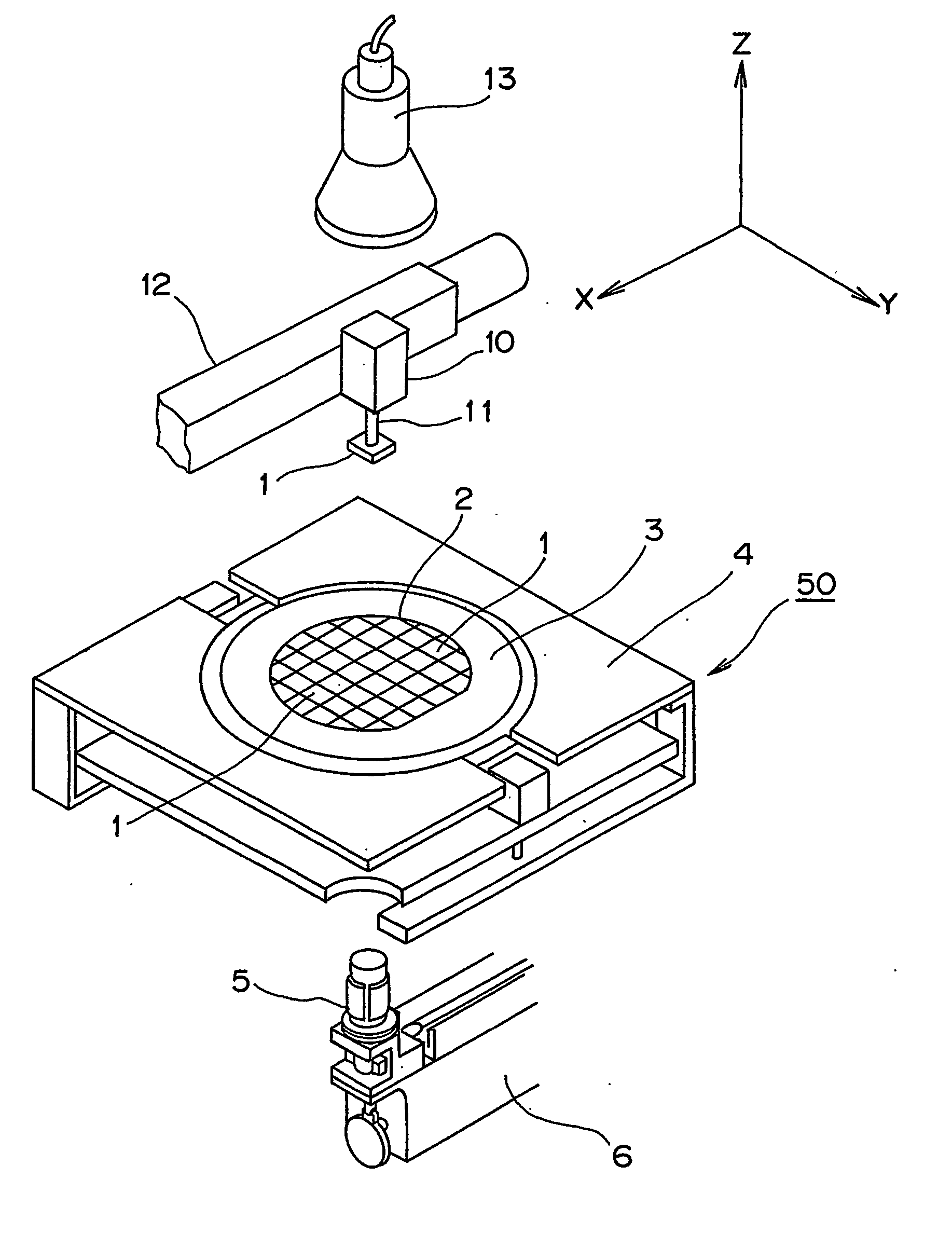
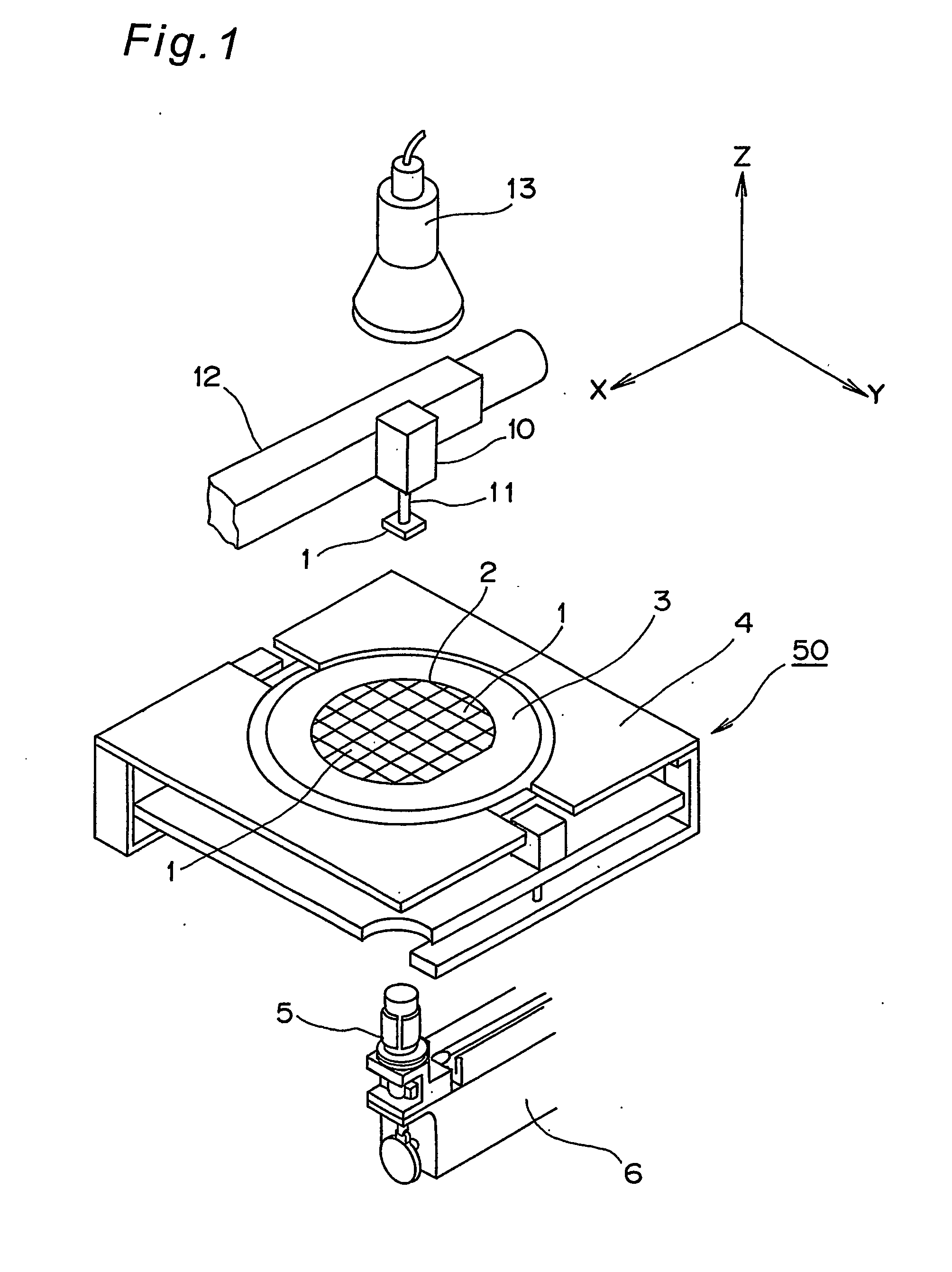
[0063]FIG. 1 is a schematic cross sectional view showing an apparatus for feeding IC-chips 50 exemplifying a semiconductor chip feeding apparatus including an apparatus for removing semiconductor chip in one embodiment of the present invention.

[0064] As shown in FIG. 1, an apparatus for feeding IC chips 50 is an apparatus in which a plurality of IC chips 1 formed from a semiconductor wafer (hereinbelow referred to as a wafer) 2 being diced is fed to, for example, a suction nozzle 11 included in a mounting head 10 in a component mounting apparatus so that the IC chips 1 are ready to be mounted on a circuit board. The IC chips 1 are IC chips which are thinner than general IC c...


PUM

PropertyMeasurementUnit
thicknessaaaaaaaaaa
thicknessaaaaaaaaaa
sizeaaaaaaaaaa

Abstract

While a vicinity of a bottom surface-side region of a pressure-sensitive adhesive sheet (3) corresponding to an adhesion region (R1) of a semiconductor chip (1) are sucked and held, a plurality of protruding portions (30) of a removing member (21) are brought into contact with the bottom surface of the semiconductor chip through the adhesive sheet at the region. Also, the adhesive sheet is sucked in between the respective protruding portions so as to change a surface bonding of the semiconductor chip to the adhesive sheet by-adhesion to a point bonding, and further the removing member is moved along the bottom surface of the semiconductor chip so as to change a position of the point bonding and decrease bonding force to the adhesive sheet by the adhesion. Then, the semiconductor chip is removed from the adhesive sheet.

Description

TECHNICAL FIELD [0001] The present invention relates to an apparatus and a method for removing semiconductor chip and an apparatus for feeding semiconductor chips, in which one out of a plurality of semiconductor chips formed from a diced semiconductor wafer is removed from a pressure-sensitive adhesive sheet that holds the semiconductor chips by adhering thereto, and the semiconductor chip is ready to be extracted (picked-up) from the pressure-sensitive adhesive sheet. BACKGROUND ART [0002] Conventionally, a plurality of semiconductor chips (hereinbelow referred to as IC chips) formed from a semiconductor wafer (hereinbelow referred to as a wafer) being diced are stored and transferred in the state of adhering to a wafer sheet (or a wafer tape) exemplifying the pressure-sensitive adhesive sheet. In order to enable one IC chip out of respective IC chips in such a state of adhering to wafer sheet to be ready to be taken out, the target IC chip is pushed up from the bottom surface of ...

Claims


Application Information

Patent Timeline
Patent Type & Authority Applications(United States)
IPC IPC(8): B65G1/133B23D59/00B23Q11/00H01L21/301H01L21/00H01L21/52H01L21/68H01L21/78H05K13/04
CPCH01L21/67132Y10T156/1132Y10T156/1944
Inventor KABESHITA, AKIRAHAMASAKI, KURAYASUMINAMITANI, SHOZOMAKINO, YOICHITANI, NORIYUKI
Owner PANASONIC CORP
Why Eureka
Try Eureka