

Substrate contact for a capped MEMS and method of making the substrate contact at the wafer level
a technology of substrate contact and capped mems, which is applied in the field of microelectromechanical systems, can solve the problems of increasing the size of the mems accelerometer, experiencing parasitic capacitance from the device during operation, and difficulty in handling and bonding the bond wir
- Summary
- Abstract
- Description
- Claims
- Application Information
AI Technical Summary
Benefits of technology
Problems solved by technology
Method used
Image

Examples
Embodiment Construction
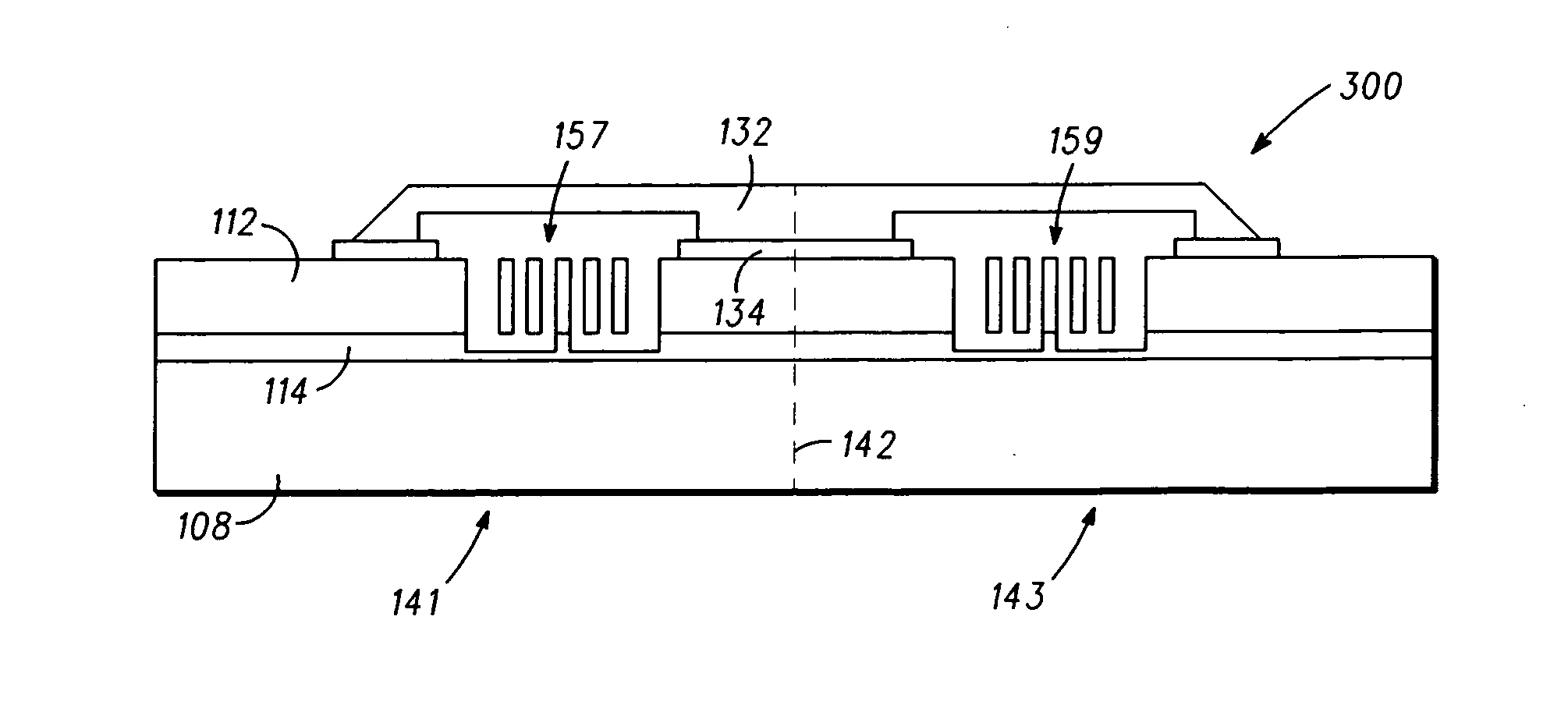
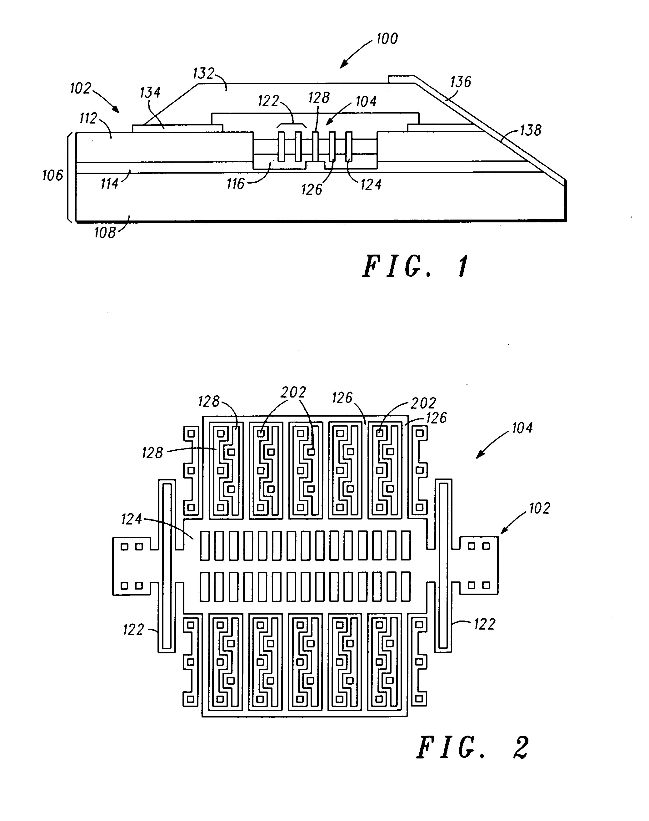
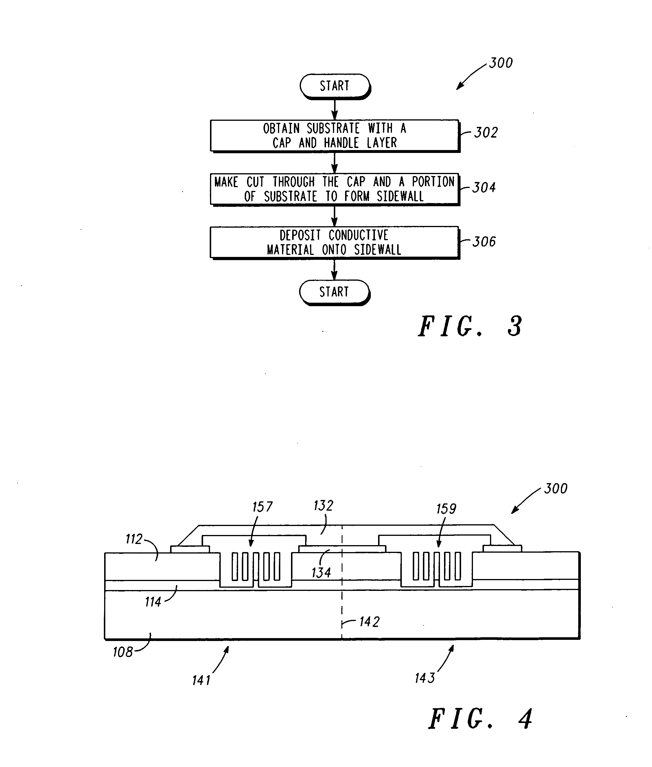
[0014] The following detailed description is merely exemplary in nature and is not intended to limit the invention or the application and uses of the invention. Furthermore, there is no intention to be bound by any expressed or implied theory presented in the preceding technical field, background, brief summary or the following detailed description. In this regard, although the invention is depicted and described in the context of an accelerometer, it will be appreciated that the invention at least could be used for any one of numerous devices that include a proof mass movably suspended above a substrate surface or any microelectromechanical systems (“MEMS”) device that may need protection from electromagnetic interference.
[0015] Turning now to the description, FIG. 1 is a cross-sectional view of an exemplary MEMS device 100. MEMS device 100 is an inertial sensor, such as an accelerometer, and includes a field region 102 and a sensor region 104 formed on a wafer 106. Wafer 106 may ...
PUM
 Abstract
Description
Claims
Application Information