

Method for manufacturing thin film transistors
- Summary
- Abstract
- Description
- Claims
- Application Information
AI Technical Summary
Benefits of technology
Problems solved by technology
Method used
Image

Examples
first embodiment
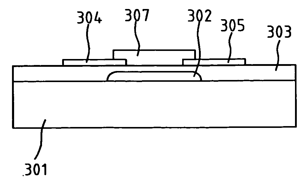
[0026] In the present invention, an inverted staggered TFT is fabricated. The manufacturing method for the staggered TFT includes the formation of a gate electrode, a gate insulator, an active channel layer, a drain electrode, and a source electrode on a substrate. FIGS. 3A-3D illustrate the manufacturing flow of an inverted staggered TFT according to the present invention. FIG. 3A is a schematic cross-sectional view of the inverted staggered TFT having a gate electrode, an insulator, an active channel, a drain electrode, and a source electrode on a substrate. Referring to FIG. 3A, it comprises the following fabrication steps. (a1) depositing a first conducting layer and patterning the first conducting layer to form a gate electrode 302 on a substrate 301. (a2) depositing and patterning a high-dielectric-constant insulating layer 303 on the gate electrode 302 and part of the substrate 301, (a3) depositing a second conducting layer and patterning the second conducting layer to form a...
second embodiment
[0029] In the present invention, a co-planar TFT is fabricated. FIGS. 4A-4D illustrate the manufacturing flow of the co-planar TFT. The manufacturing method includes photo resist patterning, surface treatment, CBD film growth, photo resist stripping, depositing and patterning an insulator, and formation of drain electrode, source electrode, and gate electrode. FIG. 4A is a schematic cross-sectional view of the co-planar TFT after photo resist patterning and surface treatment. Referring to FIG. 4A, it includes the following fabrication steps. (a1) depositing and patterning a photo resist 402 to expose an active channel on a substrate 401. (a2) doing a surface treatment to enhance the adhesion of subsequent active channel layer onto the exposed active channel. The surface treatment can be a plasma etching or a chemical reaction method to embed nanostructure catalyst onto the exposed surface.
[0030]FIG. 4B is a schematic cross-sectional view after forming an active channel layer of the ...
PUM
 Abstract
Description
Claims
Application Information