Layer Growth Using Metal Film and/or Islands

a metal film and/or island technology, applied in the direction of crystal growth process, polycrystalline material growth, chemically reactive gas, etc., can solve the problem of large lattice mismatch between nitride films and foreign substrates, difficult epitaxial nucleation on foreign substrate surfaces, and relatively large number of defects

Active Publication Date: 2006-12-21
SENSOR ELECTRONICS TECH
View PDF5 Cites 64 Cited by
  • Summary
  • Abstract
  • Description
  • Claims
  • Application Information

AI Technical Summary

Benefits of technology

[0022]FIG. 6 shows an illustrative pair of simulated band d...

Problems solved by technology

However, heteroexpitaxial grown group-III nitride films lack a native crystal nitride, which results in a large lattice mismatch between nitride films and foreign substrates.
Additionally, a large interface energy that is present due to the large lattice mismatch makes epitaxial nucleation on the foreign substrate surface difficult (“non-wetting problem”).
These shortcomings cause a relatively large number of defects and...

Method used


Image

  • Layer Growth Using Metal Film and/or Islands
  • Layer Growth Using Metal Film and/or Islands
  • Layer Growth Using Metal Film and/or Islands

Examples


Embodiment Construction

[0026] As used herein, unless otherwise noted, it is understood, that Al means Aluminum, C means Carbon, Ga means Gallium, In means Indium, N means Nitrogen, Si means Silicon, and H means Hydrogen. Further, unless otherwise noted, the term “set” means one or more (i.e., at least one) and the phrase “any solution” means any now known or later developed solution.

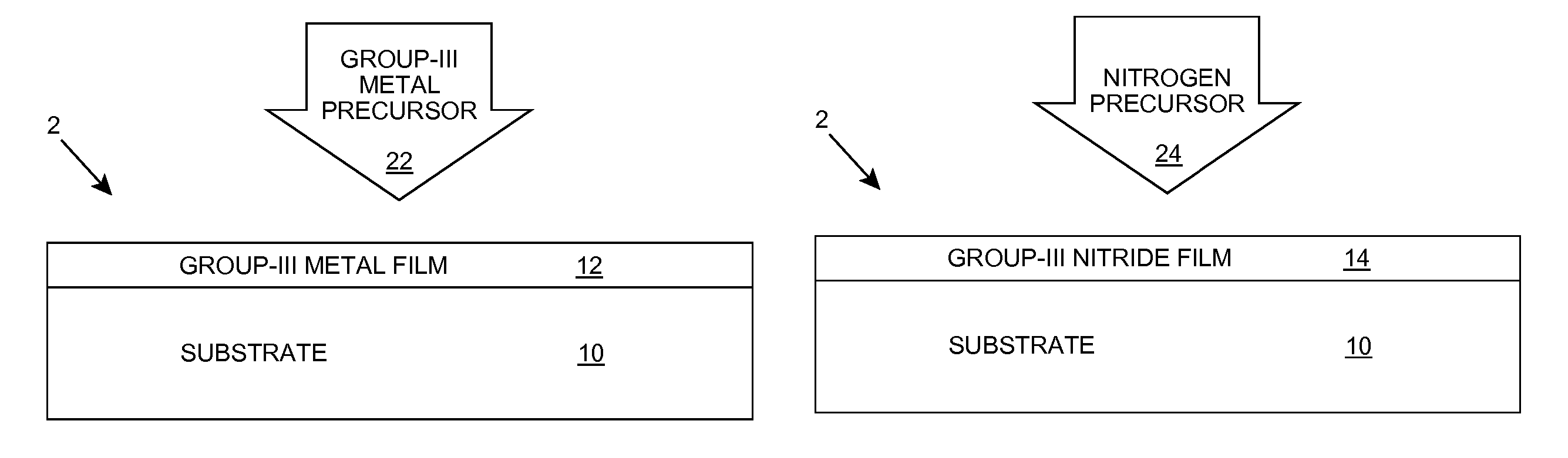
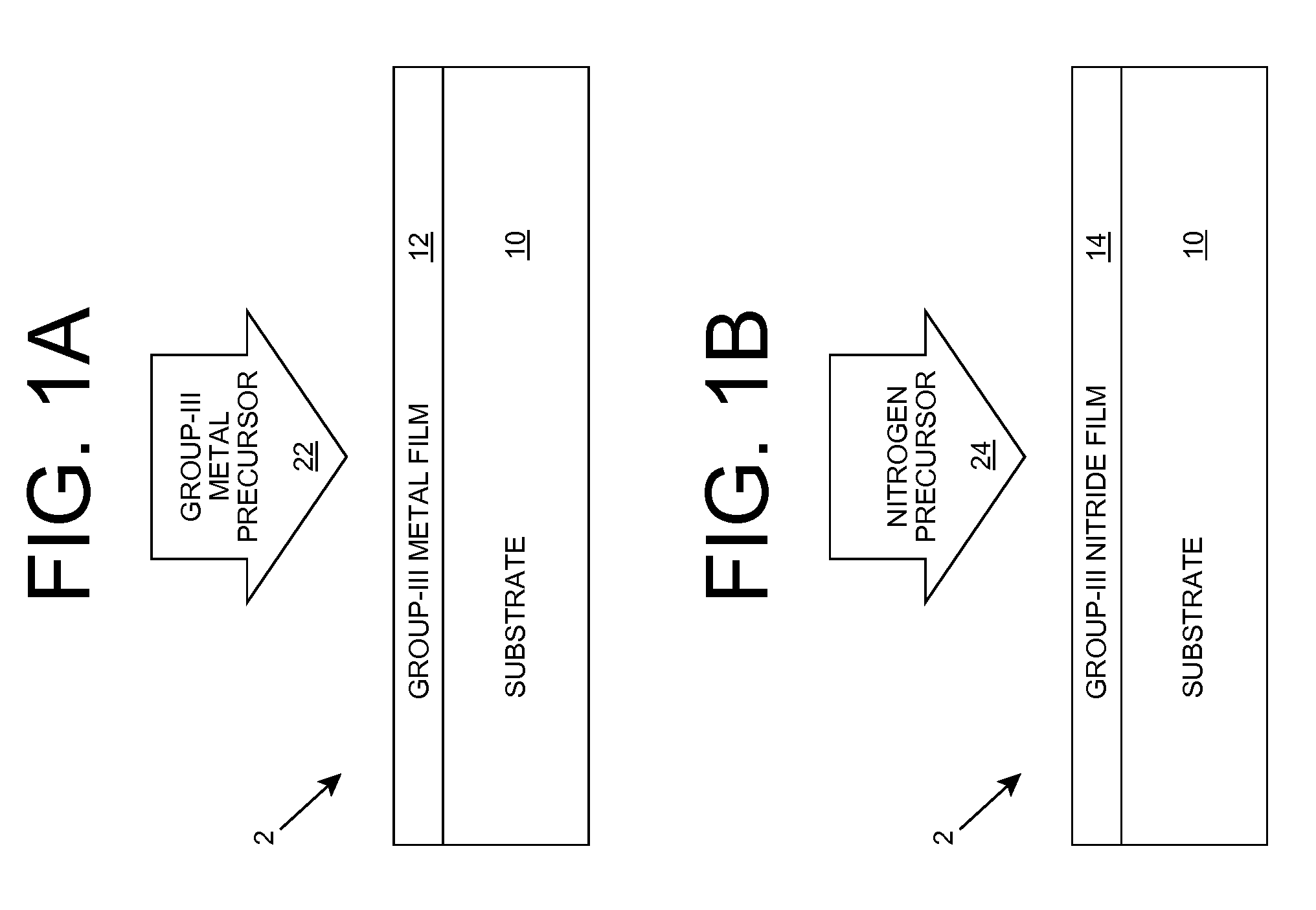
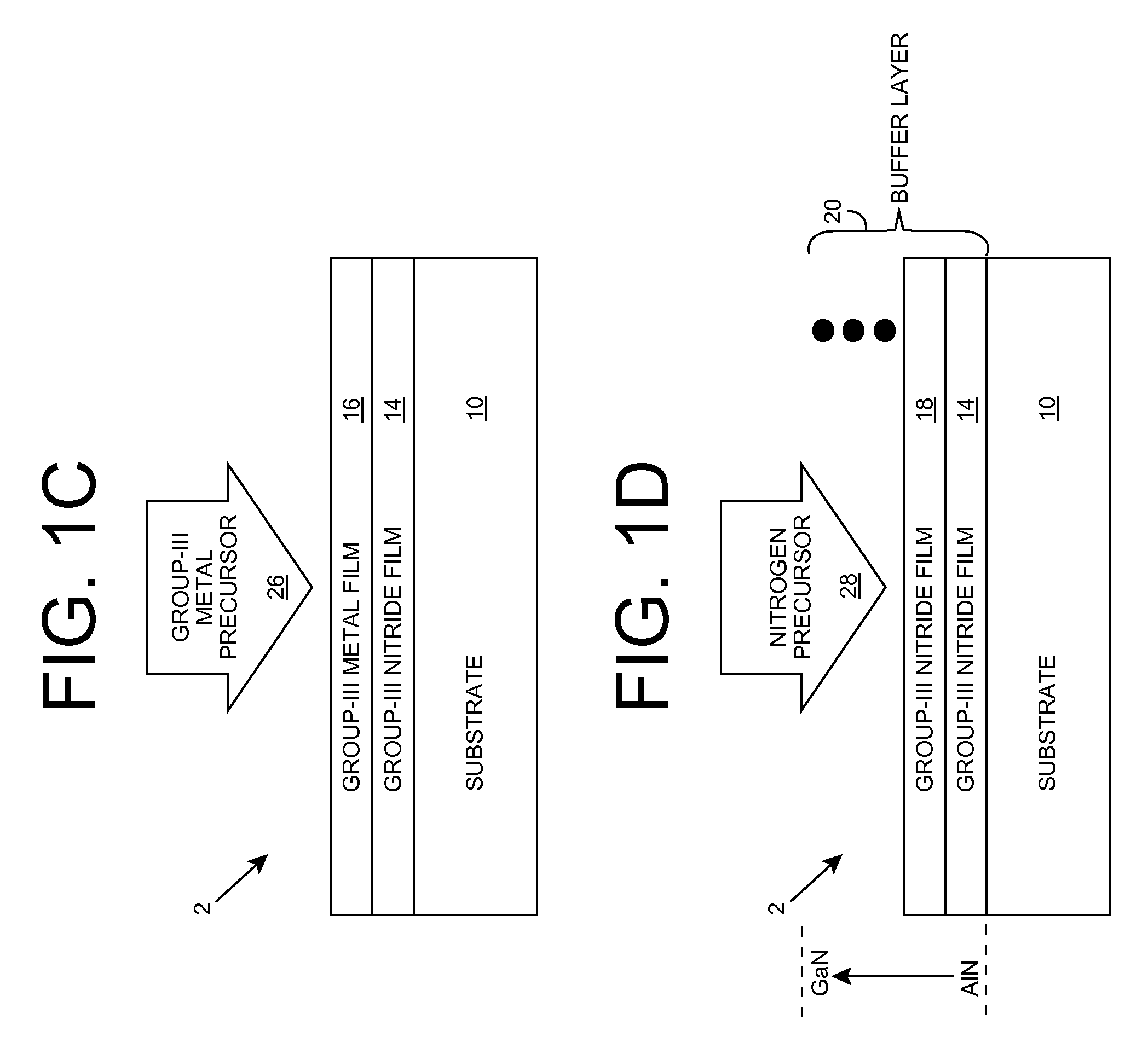
[0027] As indicated above, the invention provides a solution for manufacturing (fabricating, generating, etc.) a nitride-based heterostructure, semiconductor, device, or the like, by growing one or more layers using a metal film and / or nitride islands. In an embodiment of the invention, a group-III nitride film is grown on a surface of a lower layer. The nitride film is grown by first epitaxially growing a group-III metal film on the surface in a substantially nitrogen-free atmosphere. The group-III metal film is grown such that it covers substantially an entire area of the surface. Next, the group-III metal film is nitridate...


PUM


Abstract

A solution for manufacturing a nitride-based heterostructure, semiconductor, device, or the like, by growing one or more layers using a metal film and/or nitride islands is provided. In an embodiment of the invention, a group-III nitride film is grown on a surface of a lower layer. The nitride film is grown by first epitaxially growing a group-III metal film on the surface in a substantially nitrogen-free atmosphere. The group-III metal film is grown such that it covers substantially an entire area of the surface. Next, the group-III metal film is nitridated to form a group-III nitride film. This process can be repeated one or more times to form the layer. In another embodiment of the invention, islands are formed on a surface of a lower layer from a group-III nitride film. The islands can be used to subsequent group-III nitride growth to form the group-III nitride layer. The invention provides an improved solution for growing a layer that can be used to generate heterostructures/semiconductors/devices having improved characteristics.

Description

CROSS-REFERENCE TO RELATED APPLICATIONS [0001] The current application claims the benefit of co-pending U.S. Provisional Application No. 60 / 692,322, titled “Method for Growing Semiconductors Using A Buffer Layer”, and filed on Jun. 20, 2005, which is hereby incorporated herein by reference. The current application is related in some aspects to the co-owned, co-pending U.S. Utility Application Ser. No. 10 / 713,326, titled “Methods of Growing Nitride-Based Films Using Varying Pulses”, and filed on Nov. 14, 2003, which is hereby incorporated herein by reference.FIELD OF THE INVENTION [0002] The invention relates generally to generating a nitride-based heterostructure and a nitride-based heterostructure semiconductor, and more particularly, to a solution for growing one or more layers of the heterostructure / semiconductor using a metal film and / or islands. BACKGROUND OF THE INVENTION [0003] In general, group-III nitride semiconductors (devices) have a direct bandgap structure and a tunabl...

Claims


Application Information

Patent Timeline
IPC IPC(8): H01L21/20H01L21/36H01L31/20
CPCC30B25/02C30B29/403H01L21/0237H01L21/02458H01L21/02614H01L21/0251H01L21/0254H01L21/02584H01L21/02502
Inventor GASKA, REMIGIJUSZHANG, JIANPINGSHUR, MICHAEL
Owner SENSOR ELECTRONICS TECH
Why Eureka
Try Eureka