Method for computer aided design of semiconductor integrated circuits

a technology of integrated circuits and layout designs, applied in computer aided design, cad circuit design, instruments, etc., can solve the problems of difficult layout work, invitation to inhibit stable circuit operation, and variable transistor characteristics, and achieve excellent layout work. , the effect of stable operation of the designed semiconductor integrated circui

Inactive Publication Date: 2006-12-21
SOCIONEXT INC
View PDF3 Cites 6 Cited by
  • Summary
  • Abstract
  • Description
  • Claims
  • Application Information

AI Technical Summary

Benefits of technology

[0022] As described above, in the present invention, in generating the layer for defining the isolation region between the adjacent transistors, indexes for optimally designing the range of the layer for defining the isolation region are indicated and a layer is generated in such the optimum range by the CAD tool automatically, so that the distance from the gate electrode of the transistor to the edge of the diffusion layer (end of the isolation region defining layer) becomes optimum, thereby obtaining a desired transistor characteristic (desired amount of an electric current) and ensuring stable operation of the designed semiconductor integrated circuit excellently.

Problems solved by technology

Recently, in association with miniaturization of semiconductor elements, a problem rises that transistor characteristics vary depending on a distance from a gate electrode of a transistor to an edge of a diffusion layer.
Under the circumstances, if peripheral circuits, which are the same circuits to be layouted repeatedly depending on layout intervals of memory cells, are different from each other in the distance from the gate electrode of the transistor to the edge of the diffusion layer, circuit characteristics differ due to difference in the transistor characteristics of the peripheral circuits, resulting in invitation to inhibition of stable circuit operation.
This layout work is, however, not so easy and a desired layout cannot be obtained in some cases, reducing a design efficiency.

Method used


Image

  • Method for computer aided design of semiconductor integrated circuits
  • Method for computer aided design of semiconductor integrated circuits
  • Method for computer aided design of semiconductor integrated circuits

Examples


embodiment 1

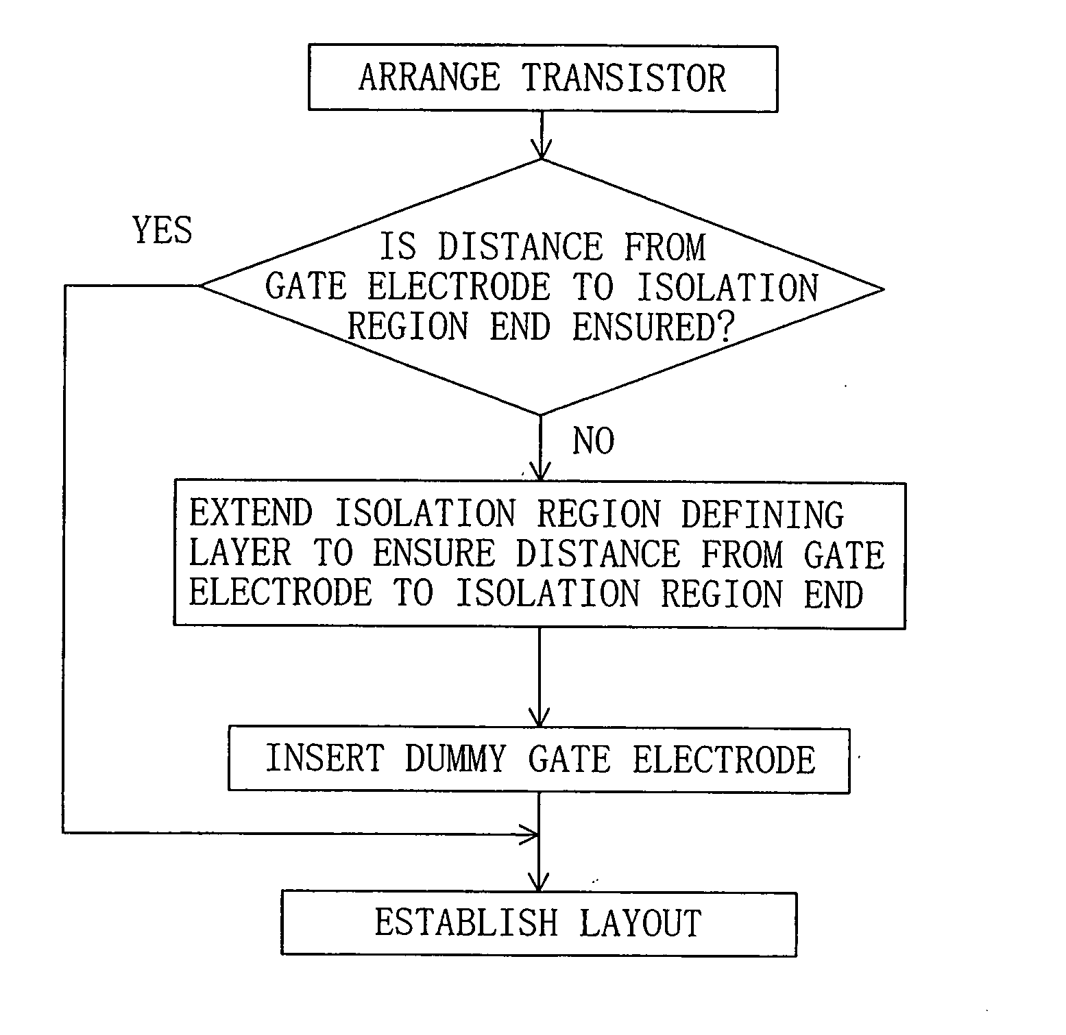
[0030]FIG. 1 is a diagram showing transistor layout generation in a method for computer aided design of a semiconductor integrated circuit in Embodiment 1 of the present invention.

[0031] A schematic constitution of the method for computer aided design of a semiconductor integrated circuit in Embodiment 1 will be described first with reference to FIG. 1. The description of the method for computer aided design of a semiconductor integrated circuit in the present embodiment will be made by referring to layout design of a MOS transistor using a CAD tool. The same is applied to Embodiment 2 and the following embodiments.

[0032] As shown in FIG. 1, elements of a MOS transistor to be layouted are generally: a layer ODA1 for defining an isolation region between adjacent transistors; and a layer GAA1 for defining a gate electrode. A region other than the layer ODA1 for defining the isolation region is to be an isolation region of a shallow trench isolation (STI). Further, an overlap region ...

embodiment 2

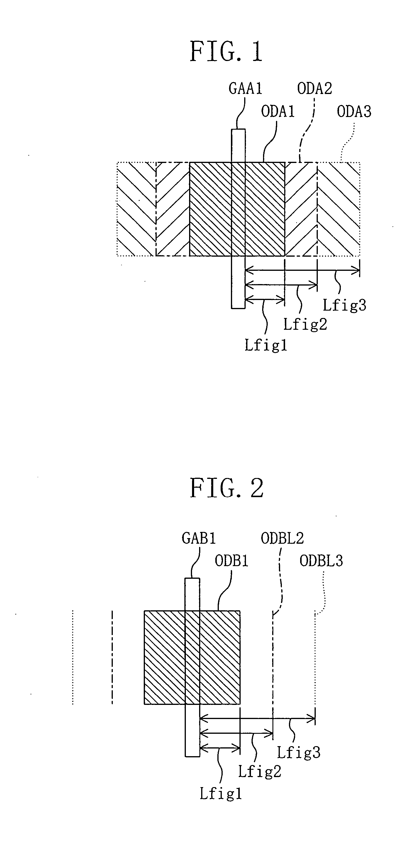
[0041]FIG. 2 is a diagram showing transistor layout generation in a method for computer aided design of a semiconductor integrated circuit in Embodiment 2 of the present invention.

[0042] A schematic constitution of the method for computer aided design of a semiconductor integrated circuit in Embodiment 2 will be described first with reference to FIG. 2.

[0043] In the method for computer aided design of a semiconductor integrated circuit in Embodiment 2, elements of a MOS transistor to be layouted are, as shown in the drawing, a layer ODB1 for defining an isolation region and a layer GAB1 for defining a gate electrode.

[0044] As shown in the drawing, distances Lfig1, Lfig2, Lfig3 from the gate electrode in the layer GAB1 for defining the gate electrode to the end of the isolation region are the finger lengths. As described above, a value of an electric current as a characteristic of a MOS transistor varies depending on the finger length. Accordingly, the finger length is desirable t...

embodiment 3

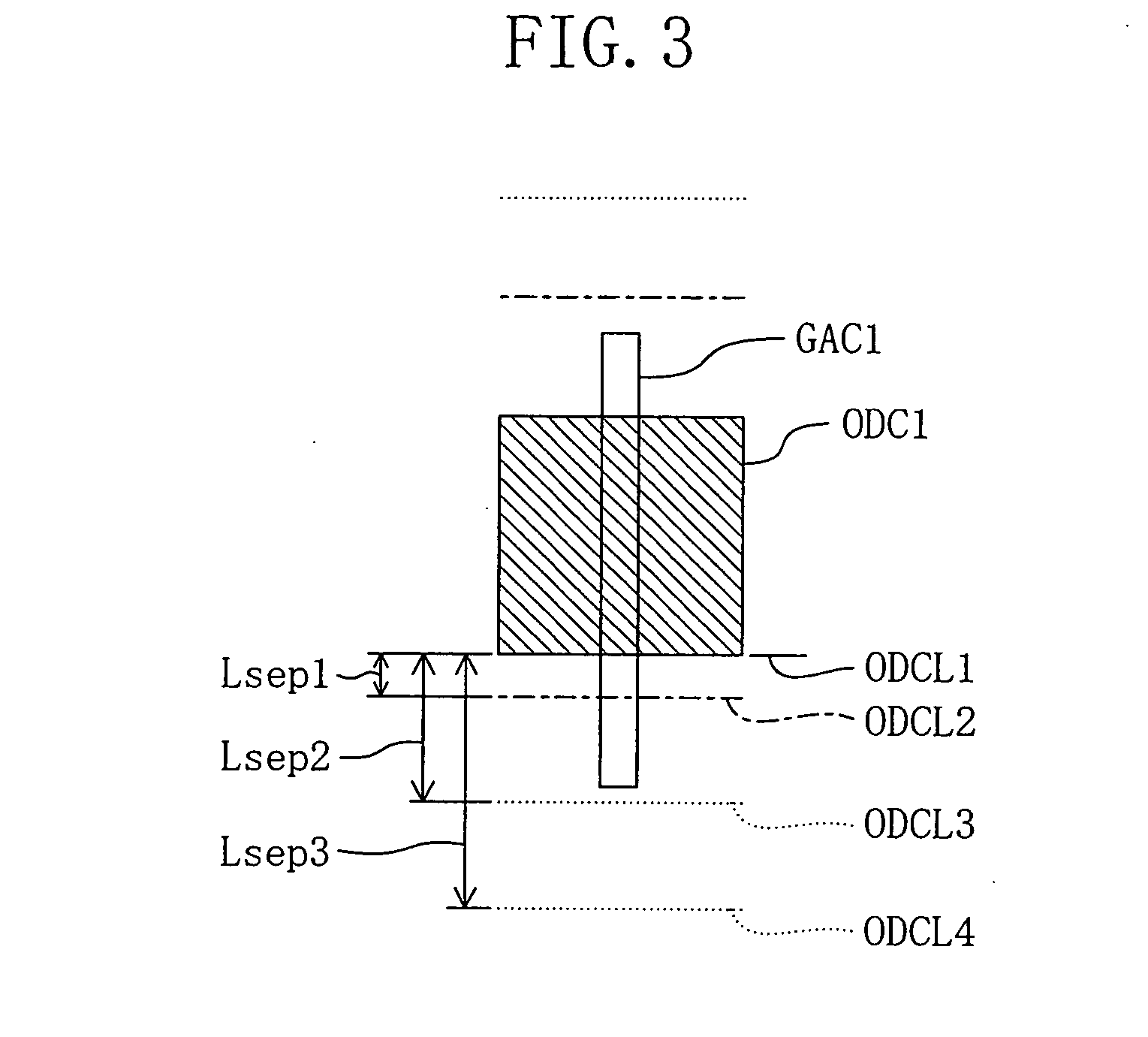
[0049]FIG. 3 is a diagram showing transistor layout generation in a method for computer aided design of a semiconductor integrated circuit in Embodiment 3 of the present invention.

[0050] A schematic constitution of the method for computer aided design of a semiconductor integrated circuit in Embodiment 3 will be described first with reference to FIG. 3.

[0051] In the method for computer aided design of a semiconductor integrated circuit according to Embodiment 3, elements to be layouted of a MOS transistor are, as shown in FIG. 3, a layer ODC1 for defining an isolation region, and a layer GAC1 for defining a gate electrode. As shown in FIG. 3, an overlap region between the layer GAC1 for defining the gate electrode and a region where ion implantation is to be performed within the layer ODC1 for defining the isolation region corresponds to the gate electrode.

[0052] As shown in the drawing, a distance from the lower end ODCL1 intersected at a right angle with the gate electrode, out...


PUM


Abstract

In transistor layout design, a plurality of distances Lfig1, Lfig2, Lfig3 from a gate electrode of a transistor to the edge of a diffusion layer are displayed by multiple lines according to a variation amount of a transistor characteristic with the use of a CAD tool. A layer for defining an isolation region between adjacent transistors is extended automatically by the CAD tool. Accordingly, even in the case where the transistor characteristic varies depending on the distance from the gate electrode of the transistor to the edge of the diffusion layer, the isolation region between the adjacent transistors can be layouted and designed optimally with no measurement of the distance by designer's visual observation necessitated.

Description

CROSS REFERENCE TO RELATED APPLICATIONS [0001] This Non-provisional application claims priority under 35 U.S.C. § 119(a) on Patent Application No. 2004-140864 filed in Japan on May 11, 2004, the entire contents of which are hereby incorporated by reference. BACKGROUND ART [0002] The present invention relates to a method for computer aided design of layout design of a semiconductor integrated circuit. [0003] Conventionally, semiconductor integrated circuits composed by integrating a plurality of transistor and wirings on a semiconductor substrate are designed using a CAD tool, as disclosed in Japanese Patent Application Laid Open Publication No. 2001-351985A, for example. [0004] Recently, in association with miniaturization of semiconductor elements, a problem rises that transistor characteristics vary depending on a distance from a gate electrode of a transistor to an edge of a diffusion layer. In a P-channel MOS transistor having a long distance from the gate electrode of the trans...

Claims


Application Information

Patent Timeline
Patent Type & Authority Applications(United States)
IPC IPC(8): G06F17/50H01L21/82H01L21/8234H01L27/02H01L27/088
CPCH01L27/0207G06F17/5068G06F30/39
Inventor SHIBAYAMA, AKINORI
Owner SOCIONEXT INC
Why Eureka
Try Eureka