CMOS image sensor

a technology of image sensor and metal oxide semiconductor, which is applied in the field of complementary metal oxide semiconductor (cmos) image sensor, can solve the problems of high dark current of cmos image sensor, and achieve the effect of reducing dark curren

Inactive Publication Date: 2006-12-28
KOREA ADVANCED INST OF SCI & TECH
View PDF0 Cites 26 Cited by
  • Summary
  • Abstract
  • Description
  • Claims
  • Application Information

AI Technical Summary

Benefits of technology

[0017] Thanks to the above-described structure, the CMOS image sensor can effectively reduce a dark current between the photodiode and the shallow trench isolati...

Problems solved by technology

However, the CMOS image sensors also have...

Method used


Image

  • CMOS image sensor
  • CMOS image sensor
  • CMOS image sensor

Examples


Embodiment Construction

[0023] Advantages and features of the present invention and methods of accomplishing the same may be understood more readily by reference to the following detailed description of preferred embodiments and the accompanying drawings.

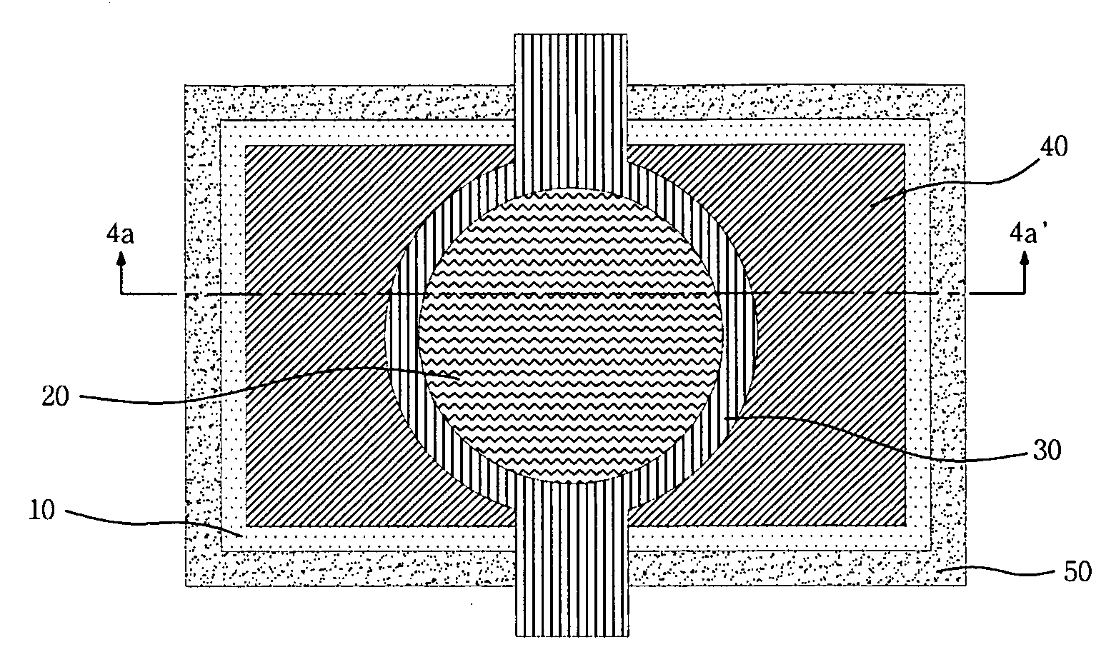
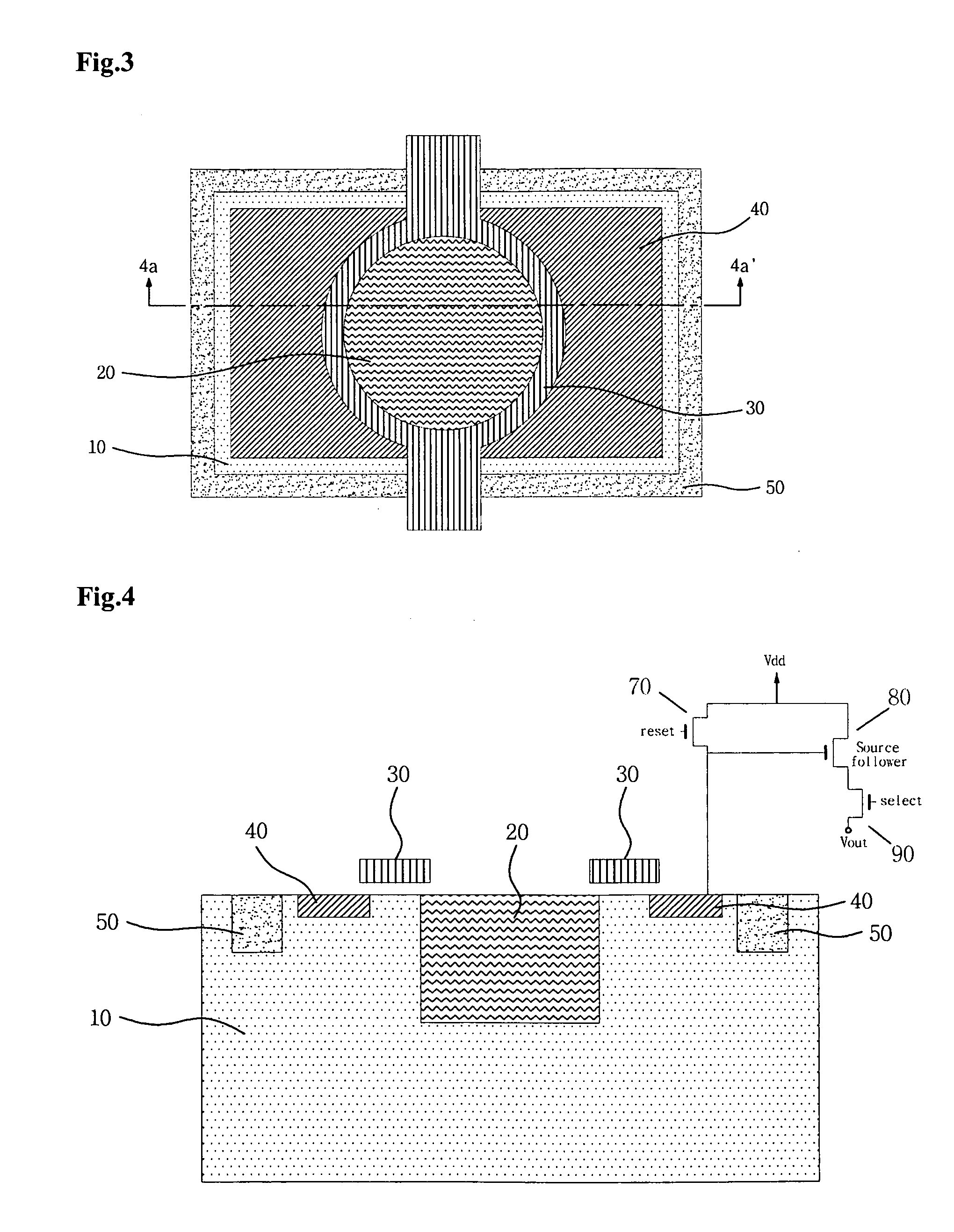
[0024] Hereinafter, a CMOS image sensor according to one embodiment of the present invention will be described with reference to FIG. 3 and FIG. 4.

[0025]FIG. 3 is a plan view illustrating a CMOS image sensor according to one embodiment of the present invention and FIG. 4 is a sectional view taken along the line 4a-4a', illustrating the CMOS image sensor according to the embodiment of the present invention.

[0026] Referring to FIG. 3 and FIG. 4, the CMOS image sensor according to one embodiment of the present invention comprises a photodiode 20 formed on a substrate for generating carriers by receiving light energy, a floating diffusion region 40 disposed in a manner such that it is distanced from the photodiode 20 and it surrounds the photodiode 20, a tr...


PUM


Abstract

Disclosed is a CMOS image sensor, comprising a photodiode formed in a substrate, a floating diffusion region formed in the substrate in a manner such that it is distanced from the photodiode surrounds the photodiode and a transfer gate formed in a manner such that it is distanced from the photodiode and the floating diffusion region and formed in a boundary area between the photodiode and the floating diffusion region, thereby overlapping the photodiode and the floating diffusion region.

Description

[0001] The present invention claims the benefit of Korean Patent Application No. 10-2005-0055015 filed in Korea on Jun. 24, 2005, which is hereby incorporated by reference. FIELD OF THE INVENTION [0002] The present invention relates to a complementary metal oxide semiconductor (CMOS) image sensor, and more particularly to a CMOS image sensor having a structure capable of effectively reducing a dark current. BACKGROUND OF THE RELATED ART [0003] Generally, CMOS image sensors are manufactured using a field effect transistor (FET) manufacturing process. The CMOS image sensor manufactured through the FET manufacturing process has advantages of consuming lower power, incurring lower cost, achieving higher degree of integration than charge-coupled device (CCD) image sensors. However, the CMOS image sensors also have the disadvantage of having a high dark current. [0004] Problems and disadvantages of the conventional CMOS image sensors will be described with reference to FIG. 1 and FIG. 2. ...

Claims


Application Information

Patent Timeline
IPC IPC(8): H01L31/113H01L27/146H04N5/335H04N5/361H04N5/369H04N5/374
CPCH01L27/14603H01L27/14643H01L27/1463H01L27/14609H01L27/146
Inventor LEE, SANG-JUNCHOI, YANG-KYUJANG, DONG-YOON
Owner KOREA ADVANCED INST OF SCI & TECH
Why Eureka
Try Eureka