Semiconductor device and method for fabricating the same

a semiconductor and upper electrode technology, applied in semiconductor devices, capacitors, electrical equipment, etc., can solve the problems of affecting the quick operation of memory cells, affecting the speed of memory cell operation, and the probability of causing failures such as breaks extremely high, so as to prevent breakage, prevent delay of start-up, and high integration

Active Publication Date: 2006-12-28
PANNOVA SEMIC
View PDF1 Cites 8 Cited by
  • Summary
  • Abstract
  • Description
  • Claims
  • Application Information

AI Technical Summary

Benefits of technology

[0011] In the conventional example described above, when a thermal treatment is performed for crystallization of the dielectric film forming the first and second BST thin films 112 and 113, a problem arises that in a portion of the capacitor upper electrode 114 located around the bottom of the concave hole and having the worst step coverage, the upper electrode 114 becomes broken depending on the selected material thereof. In addition, the capacitor upper electrode 114 is made of a platinum film for the reason that the platinum film has a good compatibility with a dielectric film such as the first and second BST films 112 and 113, and a high ductility of the capacitor upper electrode 114 made of a platinum film in turn facilitates stress migration. From this, it is obvious that such a thermal stress migration causes a high incidence of breaks in the capacitor upper electrode 114.
[0015] In view of the foregoing, an object of the present invention is to provide a highly-integrated, quickly operable dielectric memory device of a three-dimensionally stacked structure which prevents interconnect delay of a cell plate of a capacitor upper electrode without depending on the material for a dielectric material and the material for a capacitor upper electrode.
[0017] With the semiconductor device according to one aspect of the present invention, the low-resistance conductive layer is provided on the top of the capacitor upper electrode. Thus, even though the material of high resistivity such as an oxide is used as an electrode material for the capacitor upper electrode for the purpose of preventing breaks due to stress migration during a thermal treatment, start-up at the time of driving a cell plate can be prevented from delaying, thereby avoiding interconnect delay. Consequently, a capacitor element having a cell structure with no interconnect delay caused therein can be realized without depending on the material for the dielectric film and the material for the capacitor upper electrode, so that a semiconductor device capable of having a high packing density can be provided.
[0021] With this device, the capacitor upper electrode and the low-resistance conductive layer can be patterned using the same mask. Therefore, unlike the case where they are patterned separately using different masks, the necessity to consider the alignment margin of masks is eliminated, so that a semiconductor device can be provided which can attain a further miniaturization of a cell. Furthermore, the number of times masks are used decreases, so that a semiconductor device having the structure superior in mass productivity can be fabricated.
[0026] With the method for fabricating a semiconductor device according to one aspect of the present invention, even though the material of high resistivity such as an oxide is used as an electrode material for the capacitor upper electrode for the purpose of preventing breaks due to stress migration during a thermal treatment, a semiconductor device can be fabricated which can prevent delay of start-up at the time of driving a cell plate to avoid interconnect delay. Consequently, a capacitor element having a cell structure with no interconnect delay caused therein can be realized without depending on the material for the dielectric film and the material for the capacitor upper electrode, so that a semiconductor device capable of being highly integrated can be provided.
[0027] As is apparent from the above, with the semiconductor device and its fabrication method according to the present invention, the conductive layer having a lower resistance than the capacitor upper electrode is formed on the top of the capacitor upper electrode. Thereby, even in the case where the material of high resistance is used for the capacitor upper electrode for the reason of the compatibility with the dielectric film, prevention of breaks during a thermal treatment, the gap-filling capability, and the like, a highly-integrated, quickly operable semiconductor device as a dielectric memory device can be provided in which no interconnect delay is caused at the time of driving the cell plate.

Problems solved by technology

From this, it is obvious that such a thermal stress migration causes a high incidence of breaks in the capacitor upper electrode 114.
From this fact, it is conceivable that if the rise in the crystallization temperature and the long-time consumption of the crystallization proceed, the probability of causing failures such as breaks extremely rises.
That is to say, if a material of higher resistance is chosen as an oxide material for the capacitor upper electrode, interconnect delay in which start-up delays at the time of driving the cell plate occurs to hamper quick operation of a memory cell.

Method used


Image

  • Semiconductor device and method for fabricating the same
  • Semiconductor device and method for fabricating the same
  • Semiconductor device and method for fabricating the same

Examples


first embodiment

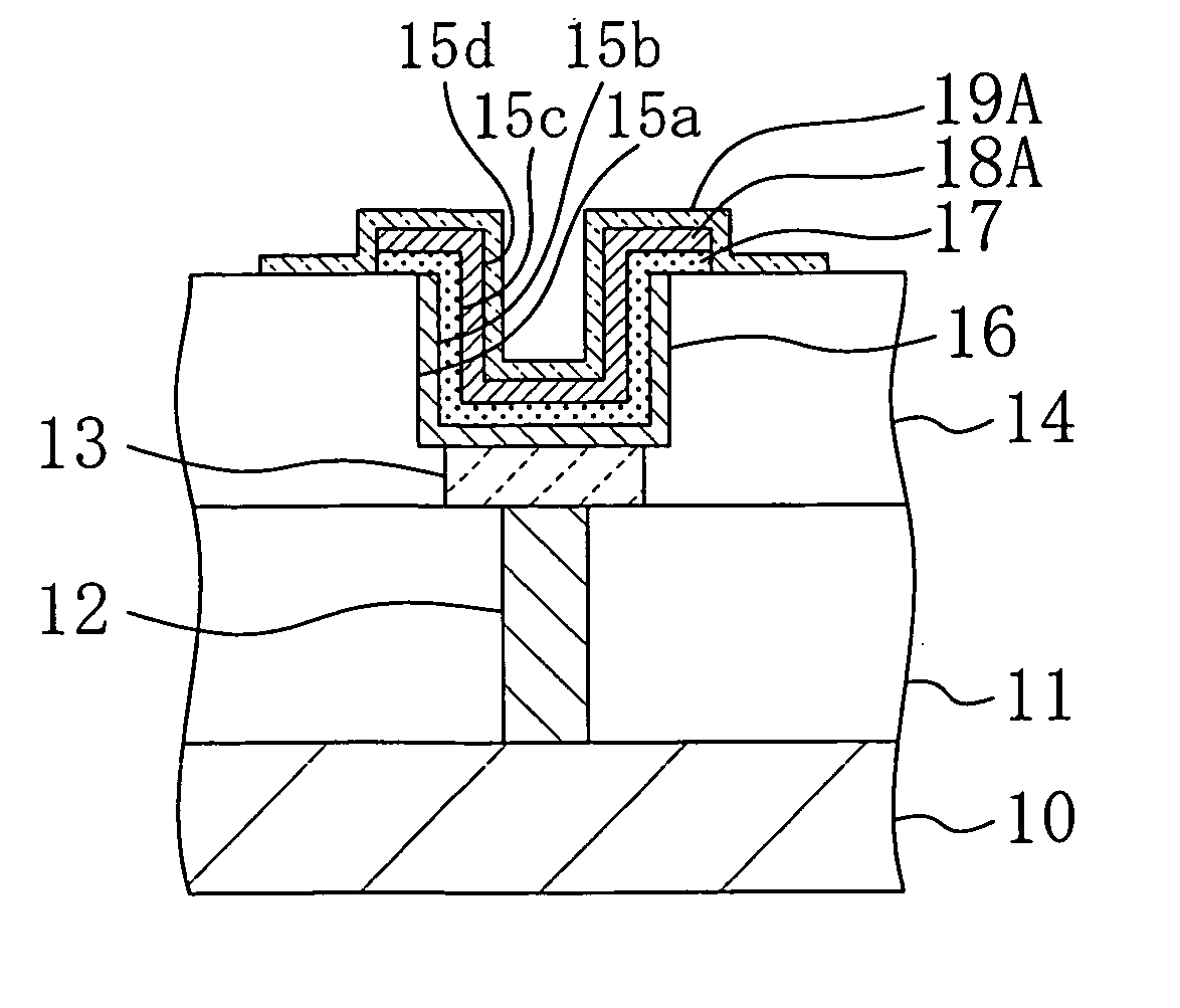
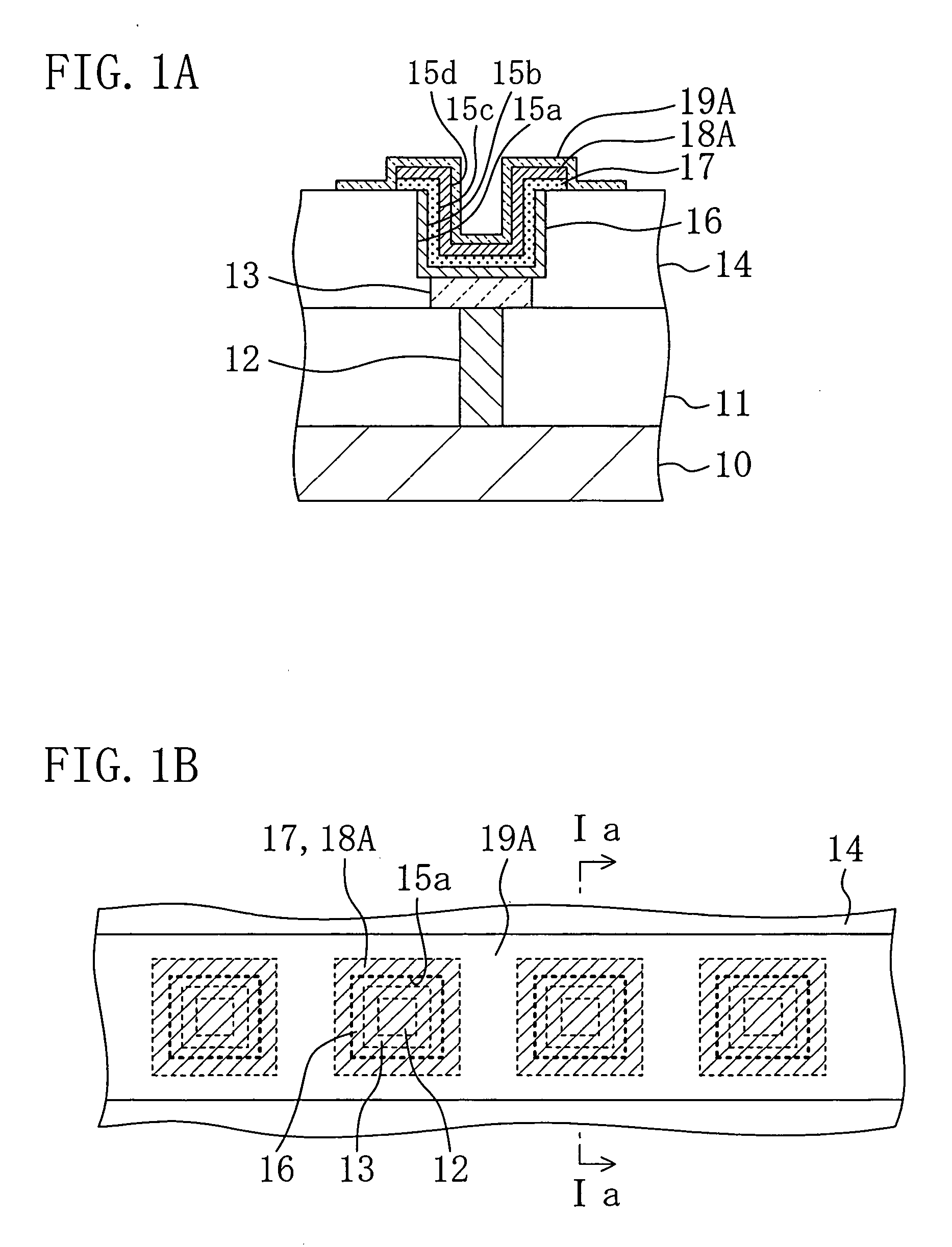
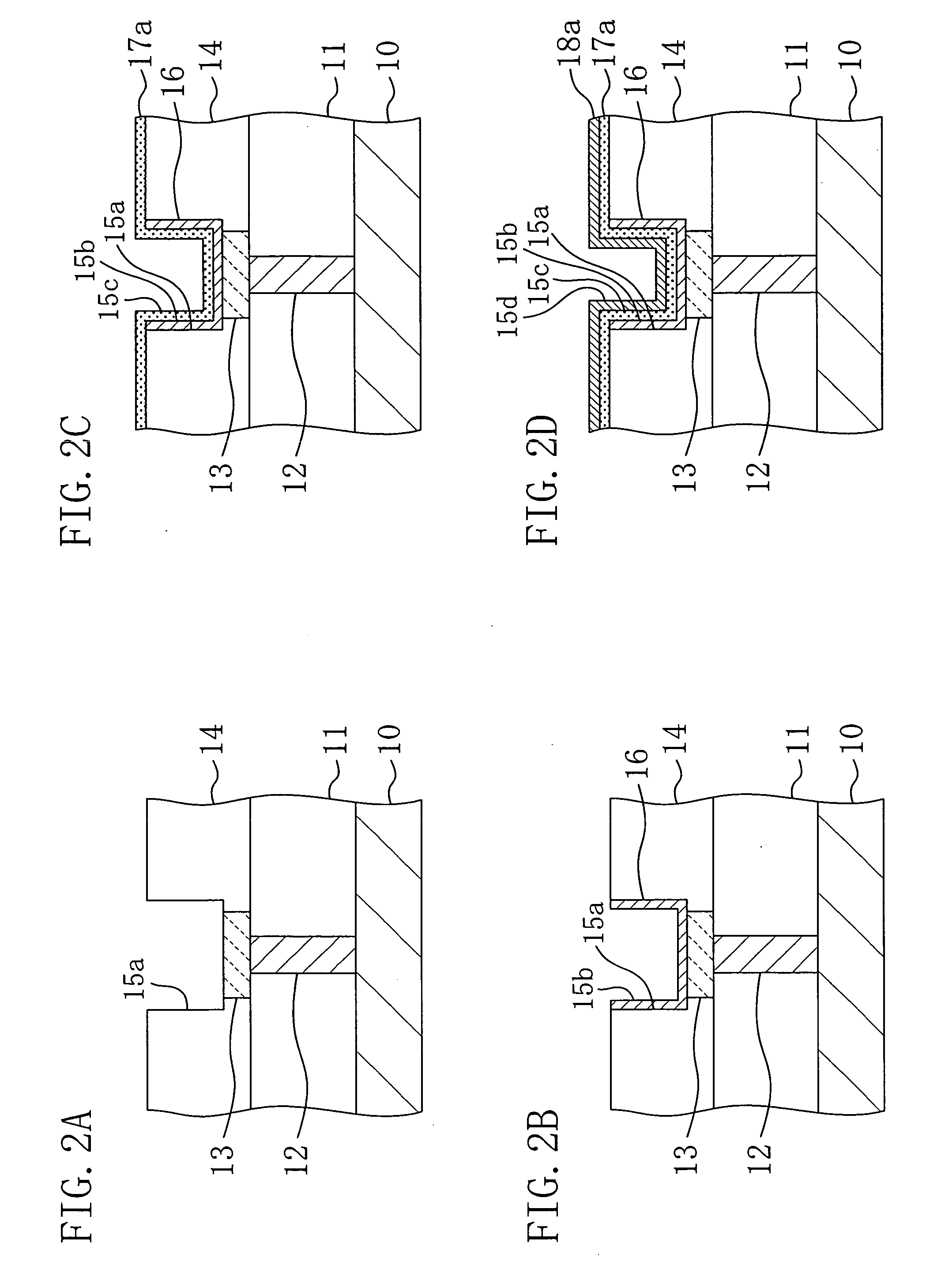
[0039] The structure of a semiconductor device according to a first embodiment of the present invention will be described below with reference to FIGS. 1A and 1B.

[0040]FIG. 1A shows the structure of the semiconductor device according to the first embodiment of the present invention, and is a sectional view taken along the line Ia-Ia in FIG. 1B. FIG. 1B is a plan view showing the structure of the semiconductor device according to the first embodiment of the present invention.

[0041] Referring to FIG. 1A, a first interlayer insulating film 11 of a silicon oxide film having 300 to 800 nm is formed on a semiconductor substrate 10. The first interlayer insulating film 11 is formed with a storage node contact 12 of a tungsten film or a polysilicon film. The storage node contact 12 penetrates the first interlayer insulating film 11 to reach an active region (not shown) of the semiconductor substrate 10. On the first interlayer insulating film 11, an oxygen barrier film 13 is formed which ...

second embodiment

[0064] Hereinafter, the structure of a semiconductor device according to a second embodiment of the present invention will be described with reference to FIGS. 4A and 4B.

[0065]FIG. 4A shows the structure of the semiconductor device according to the second embodiment of the present invention, and is a sectional view taken along the line IVa-IVa in FIG. 4B. FIG. 4B is a plan view showing the structure of the semiconductor device according to the second embodiment of the present invention.

[0066] A point of difference between the structure of the semiconductor device according to the second embodiment shown in FIGS. 4A and 4B and the structure of the semiconductor device according to the first embodiment shown in FIGS. 1A and 1B is that as shown in FIG. 4A, a capacitor upper electrode 18B is embedded to fully fill the inside of the third recess 15c. In the second embodiment, as the electrode material used for the capacitor upper electrode 18B, the material that is superior in the gap-...

third embodiment

[0078] The structure of a semiconductor device according to a third embodiment of the present invention will be described below with reference to FIGS. 7A and 7B.

[0079]FIG. 7A shows the structure of the semiconductor device according to the third embodiment of the present invention, and is a sectional view taken along the line VIIa-VIIa in FIG. 7B. FIG. 7B is a plan view showing the structure of the semiconductor device according to the third embodiment of the present invention.

[0080] A point of difference between the structure of the semiconductor device according to the third embodiment shown in FIGS. 7A and 7B and the structure of the semiconductor device according to the first embodiment shown in FIGS. 1A and 1B is that as shown in FIGS. 7A and 7B, a capacitor upper electrode 18C and a low-resistance conductive layer 19C of the third embodiment have almost the same shapes.

[0081] On the top of the capacitor insulating film 17 and the wall and bottom of the third recess 15c, th...


PUM


Abstract

A semiconductor device comprises: an insulating film formed over a semiconductor substrate and having a first recess; a plurality of capacitor elements each of which is composed of a capacitor lower electrode formed on wall and bottom portions of the first recess and having a second recess, a capacitor insulating film of a dielectric film formed on wall and bottom portions of the second recess and having a third recess, and a capacitor upper electrode formed on wall and bottom portions of the third recess; and a conductive layer (referred hereinafter to as a low-resistance conductive layer) which is formed to cover at least portions of the respective capacitor upper electrodes constituting the plurality of capacitor elements and to extend across the plurality of capacitor elements and which has a lower resistance than the capacitor upper electrode.

Description

CROSS-REFERENCE TO RELATED APPLICATIONS [0001] This application claims priority under 35 U.S.C. § 119 on Patent Application No. 2005-185314 filed in Japan on Jun. 24, 2005, the entire contents of which are hereby incorporated by reference. BACKGROUND OF THE INVENTION [0002] (a) Fields of the Invention [0003] The present invention relates to semiconductor devices which are provided with capacitor elements of three-dimensionally stacked structures employing dielectric films of dielectric materials as capacitor insulating films, and to methods for fabricating such devices. [0004] (b) Description of Related Art [0005] In development of ferroelectric memory devices, those of planar structures having small capacities of 1 to 64 kbit start being produced in volume. Recently, the center of development of the ferroelectric memory devices has been shifting to those of stack structures having large capacities of 256 kbit to 4 Mbit. In the ferroelectric memory devices of stack structures, a con...

Claims


Application Information

Patent Timeline
Patent Type & Authority Applications(United States)
IPC IPC(8): H01L21/20H01L29/00
CPCH01L27/11502H01L27/11507H01L28/91H01L28/65H01L28/55H10B53/30H10B53/00H01L27/105
Inventor MIKAWA, TAKUMINASU, TORU
Owner PANNOVA SEMIC
Why Eureka
Try Eureka