Flash Memory Device

a flash memory and endurance technology, applied in the direction of semiconductor devices, electrical devices, transistors, etc., can solve the problems of degrading data retention characteristics, generating cycle failures, and affecting so as to improve the reliability and yield of flash memory devices, improve data retention characteristics and endurance characteristics of flash memory devices

Active Publication Date: 2007-01-04
SK HYNIX INC
View PDF8 Cites 15 Cited by
  • Summary
  • Abstract
  • Description
  • Claims
  • Application Information

AI Technical Summary

Benefits of technology

[0015] Such a flash memory device may improve a data retention characteristic and an endurance characteristic of flash memory device.
[0016] Such a flash memory device may further improve the reliability and yield of flash memory device.

Problems solved by technology

It means that cycling fail is generated.
This results in a degraded data retention characteristic.
Furthermore, the larger the cycling number, the greater the amount of charges trapped in the oxide film between the control gate and the channel region.
Therefore, since a threshold voltage is shifted or breakdown is generated, cycling fail occurs.
In the related art, however, cycling fail is generated after 1K cycling.
It is considered that this causes a serious problem in the endurance characteristic of the flash memory device.

Method used


Image

  • Flash Memory Device
  • Flash Memory Device
  • Flash Memory Device

Examples


Embodiment Construction

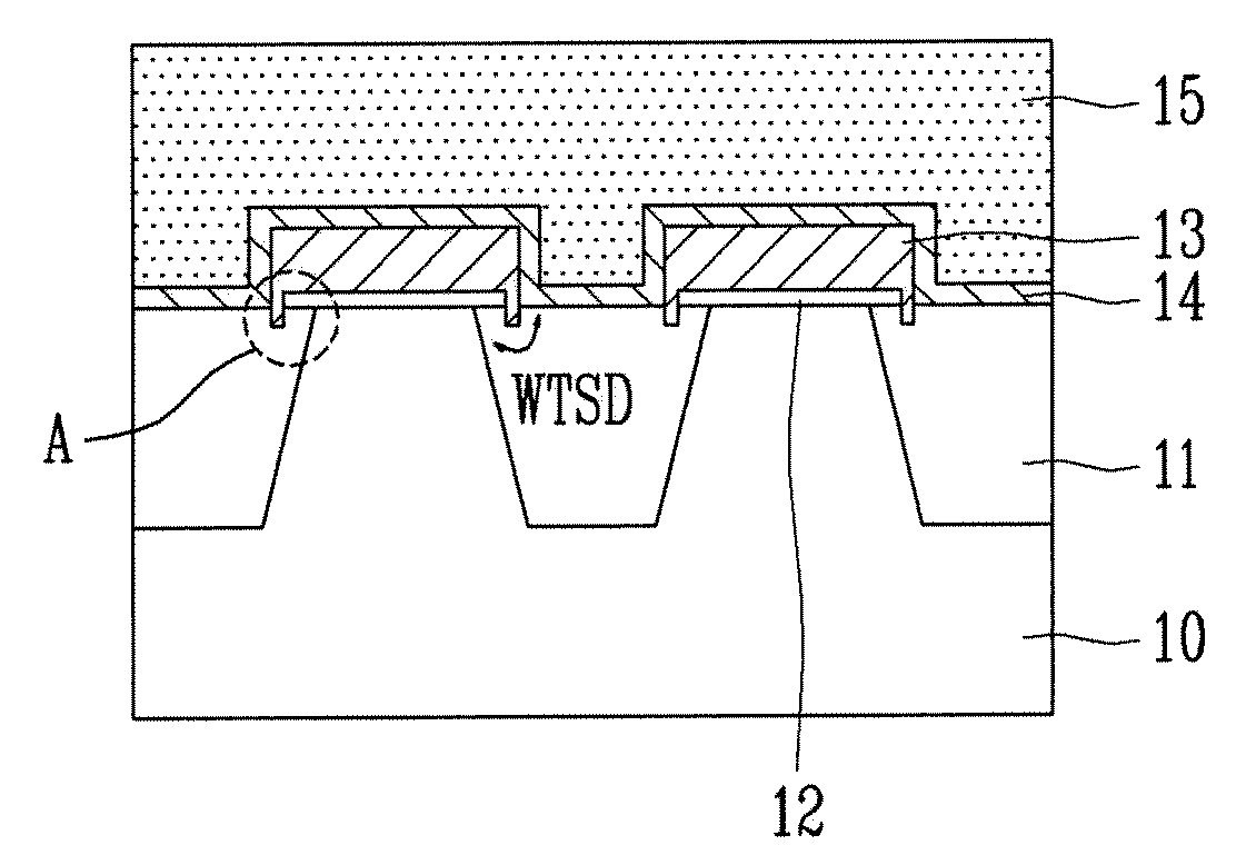
[0024]FIG. 4 is a cross-sectional view of a flash memory device according to a first described embodiment.

[0025] As shown in FIG. 4, an isolation film 11 may be formed in a predetermined region of a semiconductor substrate 10. The semiconductor substrate 10 is divided into a field region an active region. A tunnel oxide film 12 is formed on the active region and the isolation film 11 adjacent to the active region.

[0026] A moat having a predetermined depth is formed in the isolation film 11 below the tunnel oxide film 12. A floating gate 13 is formed on the tunnel oxide film 12 and the isolation film 11 at both sides of the tunnel oxide film 12 while filling the moat. The semiconductor substrate 10 of the active region below the tunnel oxide film 12 is a channel region.

[0027] The moat can be formed to a depth of the degree in which a bias applied to the control gate 15 will not have an influence on the channel region, i.e., 50 to 200 Å.

[0028] A dielectric film 14 is formed along ...


PUM


Abstract

A floating gate of a flash memory device is formed in a moat formed in an isolation film. Therefore, an electric field applied between a control gate and a channel region upon cycling can be precluded or mitigated. A distance between the control gate and the channel region is set greater than a predetermined value. Therefore, an electric field applied between the control gate and the channel region upon cycling can be mitigated. As a result, a data retention characteristic and an endurance characteristic can be improved.

Description

TECHNICAL FIELD [0001] This patent relates to flash memory devices, and more particularly, to flash memory devices with an improved endurance characteristic and an improved data retention characteristic. DISCUSSION OF RELATED ART [0002]FIG. 1 is a cross-sectional view of a flash memory device for illustrating a manufacturing method of the device in the related art. [0003] Referring to FIG. 1, a tunnel oxide film 102 and a first polysilicon layer 103 for forming a floating gate are sequentially formed on a semiconductor substrate 100. The first polysilicon layer 103 and the tunnel oxide film 102 are patterned by a Self-Aligned Shallow Trench Isolation (SA-STI) method. An isolation film 104 is then formed in an isolation region. [0004] If the isolation film 104 is formed by the SA-STI method as described above, the tunnel oxide film 102 and the first polysilicon layer 103 remain on the active region between the projections of the isolation film 104 while the top of the isolation film ...

Claims


Application Information

Patent Timeline
Patent Type & Authority Applications(United States)
IPC IPC(8): H01L29/788H01L21/336
CPCH01L21/28273H01L27/115H01L29/7881H01L29/42336H01L29/66825H01L27/11521H01L29/40114H10B69/00H10B41/30
Inventor LEE, KEUN WOO
Owner SK HYNIX INC
Why Eureka
Try Eureka