Light-emitting device, circuit for driving the same, and electronic apparatus

a technology of light-emitting elements and circuits, applied in static indicating devices, instruments, electroluminescent light sources, etc., can solve the problems of different brightness levels of light-emitting elements, and achieve the effect of high accuracy

Inactive Publication Date: 2007-01-04
SEIKO EPSON CORP
View PDF9 Cites 24 Cited by
  • Summary
  • Abstract
  • Description
  • Claims
  • Application Information

AI Technical Summary

Benefits of technology

[0007] An advantage of some aspects of the invention is that it provides a technique capable of making a light emitting element emit light having a predetermined brightness with high ac

Problems solved by technology

Therefore, this structure has a problem in that the brightness le

Method used


Image

  • Light-emitting device, circuit for driving the same, and electronic apparatus
  • Light-emitting device, circuit for driving the same, and electronic apparatus
  • Light-emitting device, circuit for driving the same, and electronic apparatus

Examples


first embodiment

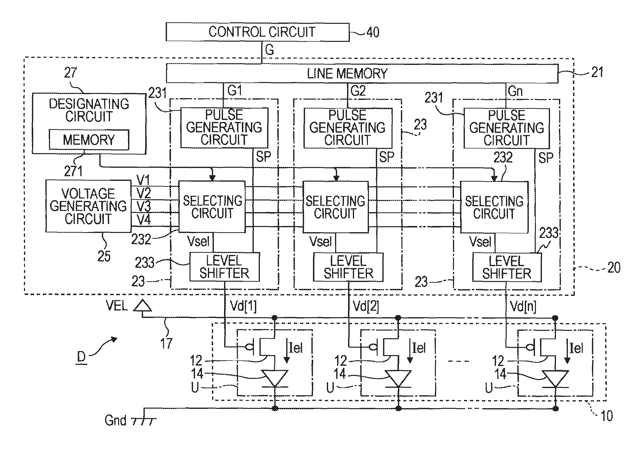
[0028]FIG. 1 is a block diagram illustrating the structure of a light emitting device according to a first embodiment of the invention. A light emitting device D of this embodiment is used as an exposure head for exposing a photoreceptor in an image forming apparatus (a printing apparatus) which forms a latent image by exposing the photoreceptor. As shown in FIG. 1, the light emitting device D includes a light emitting unit 10 having n unit circuits U (n is a natural number) arranged in a row along a scanning line, a driving circuit 20 for driving the unit circuits U, and a control circuit 40 for controlling the operation of the driving circuit 20.

[0029] Each of the n unit circuits U forming the light emitting unit 10 includes a driving transistor 12 and a light emitting element 14. The light emitting element 14 is a current driven type element for emitting light having brightness corresponding to a driving current Iel. For example, the light emitting element 14 is an OLED element ...

second embodiment

[0049] Next, a second embodiment of the invention will be described below.

[0050] In the first embodiment, contents to be designated by the designating circuit 27 is previously determined according to the characteristic value of each of the driving transistors 12 which is measured, for example, before the shipment of the light emitting device D. In contrast, in the second embodiment, contents to be designated by the designating circuit 27 (that is, the voltage Vsel output from each of the selecting circuits 232) is changed whenever necessary according to the actual usage environment of a light emitting device D. Further, in the second embodiment, the same components as those in the first embodiment have the same reference numerals, and thus a description thereof will be omitted for the purpose of simplicity.

[0051]FIG. 4 is a block diagram illustrating the structure of the light emitting device D according to the second embodiment of the invention. The light emitting device D includ...

first modification

[0063] The structures of the components shown in FIG. 1 arbitrarily change. For example, each of the signal processing circuits 23 may be formed in a structure shown in FIG. 5. The signal processing circuit 23 shown in FIG. 5 (in this modification, an i-th signal processing circuit 23 is given as an example) includes a selecting circuit 235, a switch SWb, and a control circuit 236. In the structure shown in FIG. 5, the designating circuit 27 shown in FIG. 5 is omitted from the signal processing circuit 23.

[0064] The selecting circuit 235 includes four switches SWa corresponding to voltages V1 to V4. One end of each of the switches SWa is connected to a common output terminal Tout for a data signal Vd[i]. The other ends of the switches SWa are connected to wiring lines through which the voltages (V1 to V4) corresponding to the switches SWa are supplied. Meanwhile, one end of the switch SWb is connected to a power line through which a power supply voltage VEL is supplied, and the oth...


PUM


Abstract

A light emitting device includes: a plurality of unit circuits each of which includes a driving transistor for generating a driving current corresponding to a potential of a gate and a light emitting element for emitting light having a brightness corresponding to the driving current; a plurality of signal processing units which correspond to the unit circuits; and a designating unit which designates voltages to the signal processing units. Each of the plurality of signal processing units includes: a voltage adjusting unit which variably outputs a voltage to operate the driving transistor in a saturated region in response to a designation by the designating unit; and an output unit which outputs the voltage output from the voltage adjusting unit to the gate of the driving transistor corresponding to the signal processing unit at a time density corresponding to a gray-scale value designated to the light emitting element.

Description

[0001] This application claims priority from JP 2005-194641, filed in the Japanese Patent Office on Jul. 4, 2005, the entire disclosure of which is hereby incorporated by reference in its entirety. BACKGROUND [0002] 1. Technical Field [0003] The present invention relates to a technique for controlling the driving of a light emitting element, such as an organic light emitting diode (hereinafter, referred to as an ‘OLED’). [0004] 2. Related Art [0005] There has been proposed a technique for controlling a period of time for which a light emitting element emits light to control the gray-scale level of the light emitting element. For example, JP-A-2002-108285 (see FIG. 1) discloses a display device in which light emitting elements and n-channel transistors (hereinafter, referred to as ‘driving transistors’), each having a source connected to an anode of the light emitting element, are arranged in a matrix. In such a structure, an ON voltage (a voltage to turn on the driving transistor) i...

Claims


Application Information

Patent Timeline
IPC IPC(8): G09G3/30H05B44/00
CPCG09G3/2014G09G3/3233G09G3/3291G09G2300/08G09G2300/0876G09G2320/048G09G2320/0233G09G2320/041G09G2320/043G09G2320/045G09G2310/0289G09G3/30G09G3/32G09G1/12G09G3/22
Inventor JO, HIROAKI
Owner SEIKO EPSON CORP
Why Eureka
Try Eureka