I/O circuitry for reducing ground bounce and VCC sag in integrated circuit devices

a technology of integrated circuit devices and circuits, which is applied in the direction of pulse techniques, instruments, computations using denominational number representations, etc., can solve the problems of increasing clock speeds and number of i/o pins, noise in ic devices caused by ground bounce and vcc sag becoming more of a problem, and the design of digital integrated circuit devices is unavoidably encountered, so as to reduce ground bounce and vcc sag in digital designs, reduce ground boun

Inactive Publication Date: 2007-01-11
ALTERA CORP
View PDF4 Cites 73 Cited by
  • Summary
  • Abstract
  • Description
  • Claims
  • Application Information

AI Technical Summary

Benefits of technology

[0005] In accordance with the present invention, I/O circuitry with via-programmability is provided for reducing ground bounce and VCC sag in digital designs. In particular, programmable via sites are created around I/O pins so as to be able to programmably connect the I/O pins to an I/O driver, or to create a substantially direct connection between the I/O pins and a ground or power signal of an IC device. To reduce ground bounce, unused I/O pins are coupled to board ground signal corresponding the ground signal of the PCB of the IC device, and are then directly connected to a ground conductor carrying the device ground signal using a via connection. Similarly, to reduce VCC sag, unused I/O pins are coupled to a board VCC signal c

Problems solved by technology

Ground bounce and VCC sag are two well-known analog phenomena that are unavoidably encountered in the design of digital integrated circuit devices.
The noise in IC devices caused by ground bounce and VCC sag have become more of a problem in modern semiconductor devices, which are characterized by ever-increasing clock speeds and numbers of I/O pins.
Due to such aberrations in dev

Method used


Image

  • I/O circuitry for reducing ground bounce and VCC sag in integrated circuit devices
  • I/O circuitry for reducing ground bounce and VCC sag in integrated circuit devices
  • I/O circuitry for reducing ground bounce and VCC sag in integrated circuit devices

Examples


Embodiment Construction

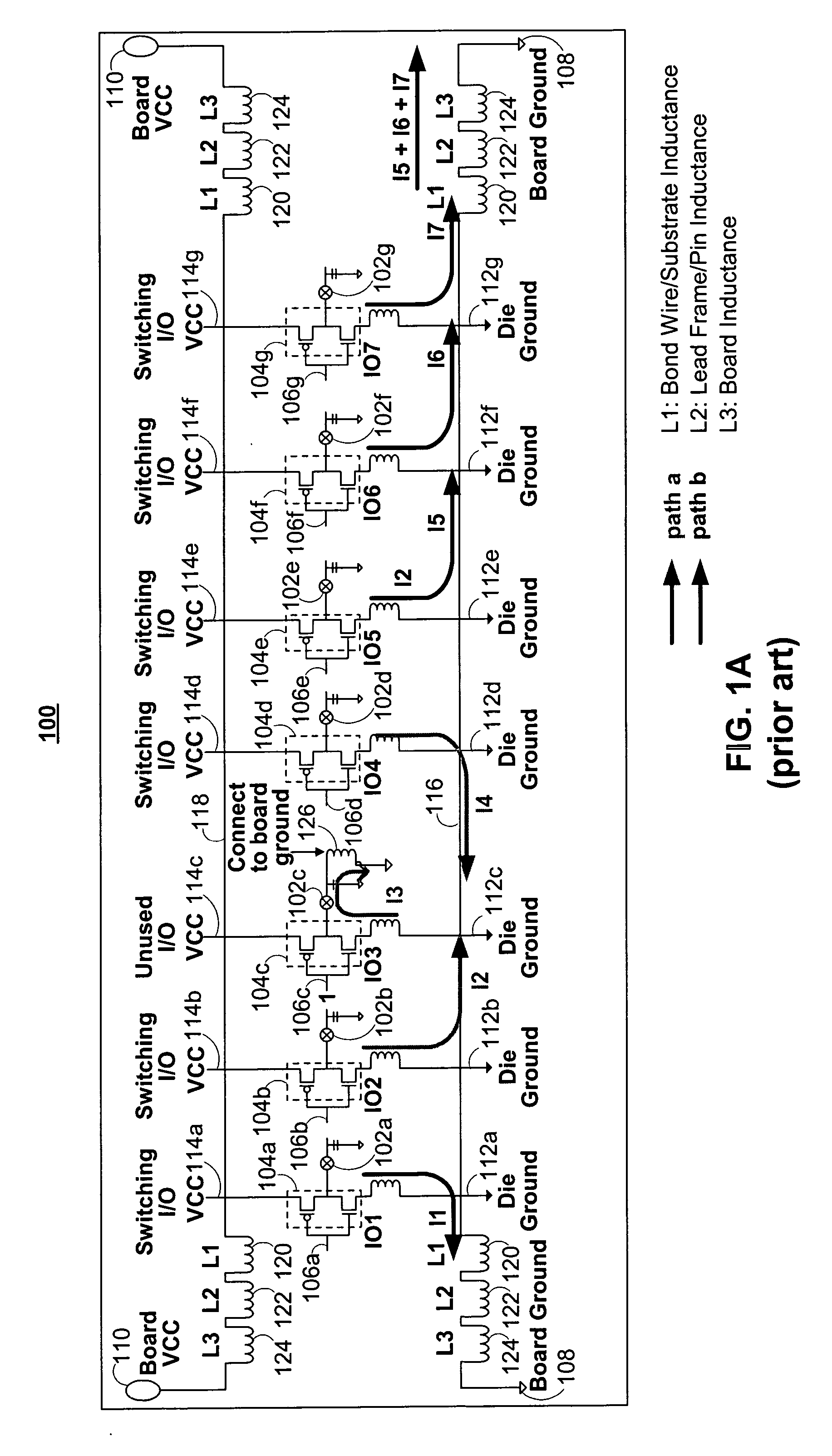
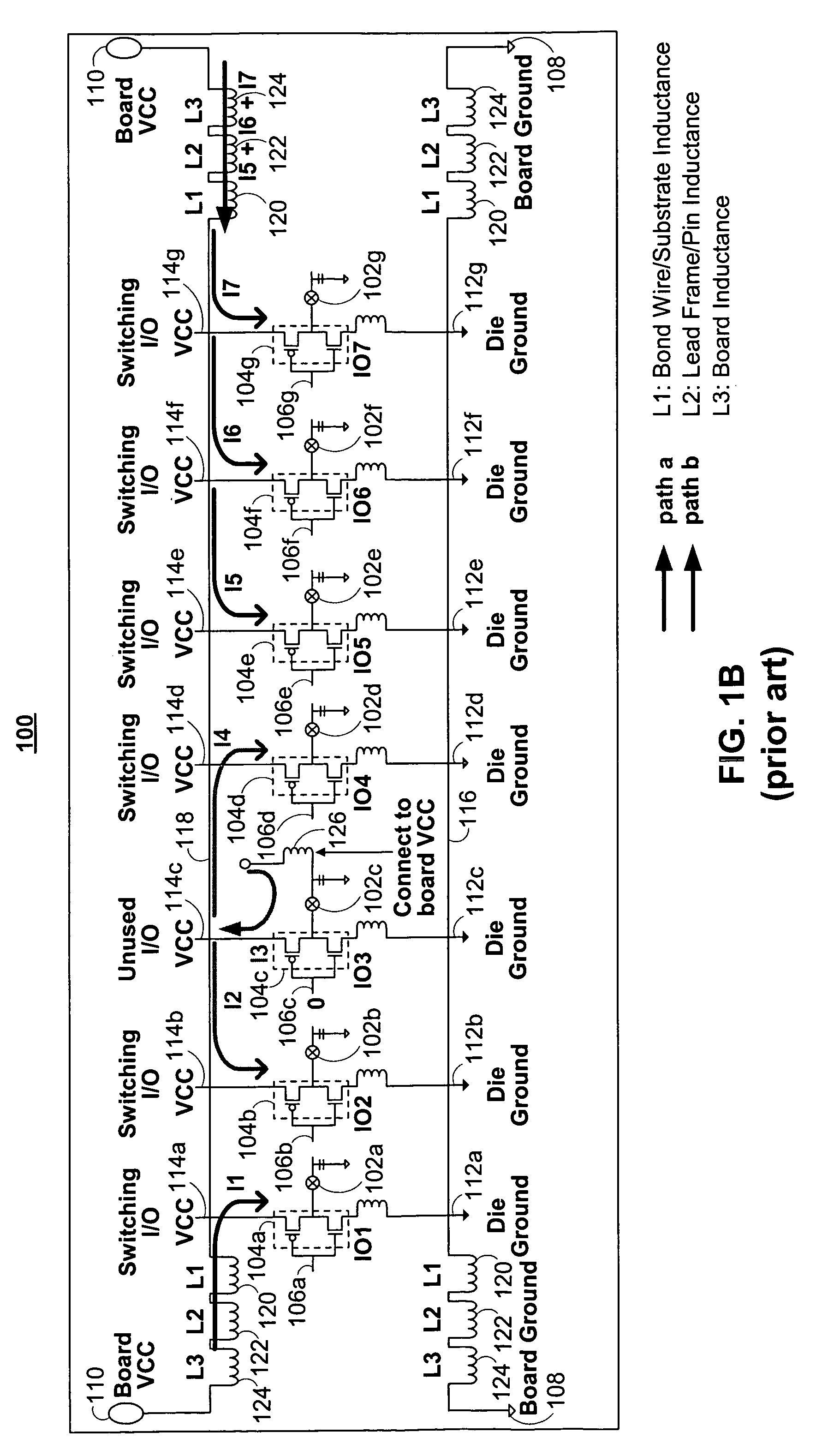
[0009]FIGS. 1A and 1B show an illustrative circuit for implementing a prior-art method for reducing ground bounce and VCC sag. In particular, FIGS. 1A and 1B show a series of seven I / O pins 102a-g of IC device 100. With the exception of I / O pin 102c, it is assumed that each of I / O pins 102a-g in FIGS. 1A and 1B is connected to an actively switching I / O data signal and is therefore being used. As a result, each of the used I / O pins is a source of ground bounce and VCC sag as previously described. I / O pin 102c is assumed to be unused for the purpose of illustrating the prior-art method for reducing ground bounce and VCC sag as will be seen below.

[0010] In FIGS. 1A and 1B, each of I / O pins 102a-g has an associated one of I / O drivers 104a-g (which may be implemented as a CMOS inverter as shown) that is used to help drive a logic signal on the corresponding I / O pin to board ground 108 or board VCC 110 depending on the logic state of the I / O pin. For instance, when the data signal connec...


PUM


Abstract

Methods and circuitry for reducing ground bounce and VCC sag effects in integrated circuit (“IC”) devices is provided. In particular, a via-programmable design for I/O circuitry in IC devices is provided. The via-programmable I/O circuitry is used to disconnect I/O pin driver circuitry from and create a substantially direct connection between unused I/O pins and the ground and/or VCC signals of an IC device to reduce ground bounce and VCC sag, respectively.

Description

BACKGROUND OF THE INVENTION [0001] This invention relates generally to I / O circuitry in integrated circuit (“IC”) devices. In particular, this invention relates to a via-programmable design for I / O circuitry in IC devices that reduces the amount of ground bounce and power (i.e., “VCC”) sag of such devices. [0002] Ground bounce and VCC sag are two well-known analog phenomena that are unavoidably encountered in the design of digital integrated circuit devices. Substantial ground bounce arises when the data signals on numerous active I / O pins on an IC device simultaneously switch from a logic 1 to a logic 0. Due to the sudden transition in the logic signals, a sudden rush of excess current (that was previously stored in the load capacitors of the I / O pins) flows from each of the I / O pins to the ground of the IC device. And since the return current path for the excess current includes several inductances (e.g., a bond wire / substrate inductance, a lead frame / pin inductance, and a board i...

Claims


Application Information

Patent Timeline
IPC IPC(8): H03K17/16
CPCH03K19/00346
Inventor LEE, ENG HUATLOO, KOK WENG
Owner ALTERA CORP
Why Eureka
Try Eureka