A pcb design method for suppressing plane resonance
A design method and planar technology, applied in the electronic field, can solve the problems of increasing design cost and increasing the difficulty of PCB design, and achieve the effects of reducing design cost, reducing ground bounce effect, and avoiding electromagnetic radiation
- Summary
- Abstract
- Description
- Claims
- Application Information
AI Technical Summary
Problems solved by technology
Method used
Image
Examples
Embodiment 1
[0020] A PCB design method to suppress plane resonance In the design of printed circuit boards, the method of changing the plane cutting is used to change the cavity formed between the power layer and the ground layer (or the power layer and the power layer), thereby improving the frequency band we focus on. resonance.
Embodiment 2
[0022] On the basis of Embodiment 1, the method of changing the plane cutting described in this embodiment is that if a resonant frequency point with the same frequency as the signal in the wiring area appears in a certain area, the power layer adjacent to this area is hollowed out for design , the hollowed-out area has the same size as the resonance area.
Embodiment 3
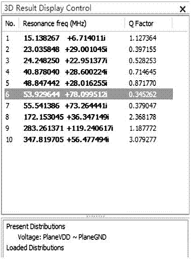
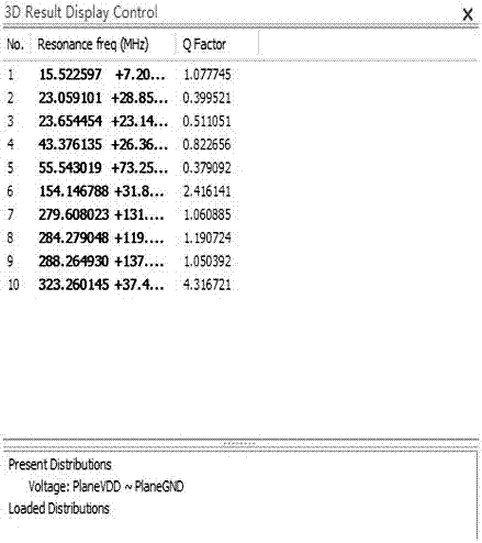
[0024] On the basis of Embodiment 1 or 2, in this embodiment, the frequency point resonance distribution of the planar resonator can be viewed through the SIGRITY POWER SI simulation software.
PUM
 Abstract
Description
Claims
Application Information

