

Optical imaging system
- Summary
- Abstract
- Description
- Claims
- Application Information
AI Technical Summary
Benefits of technology
Problems solved by technology
Method used
Image

Examples
embodiment 1
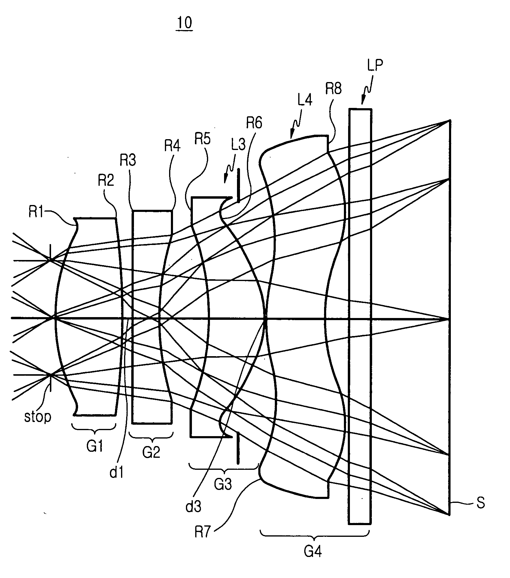
[0040] The aspheric surfaces of the lenses constituting the optical imaging system according to the first embodiment are as presented in Table 4. The spherical surfaces and other conditions are as indicated in Table 1. The aspheric surfaces can be determined according to formula (9). The optical imaging system 10 according to the first embodiment includes a first lens group G1 having a positive refractive power, a second lens group G2 having a negative refractive power, a third lens group G3 having a positive or negative refractive power, a fourth lens group G4 having a positive or negative refractive power, a stop, and a thin film filter or an optical filter.
[0041] The stop is located on the incidence side of the optical imaging system 10, and the introduced light is output to the first lens group G1. The stop is used to regulate the amount of the light introduced into the optical imaging system 10, and is separated from the first lens group G1 by 0.097005 mm.
[0042] The first len...
embodiment 2
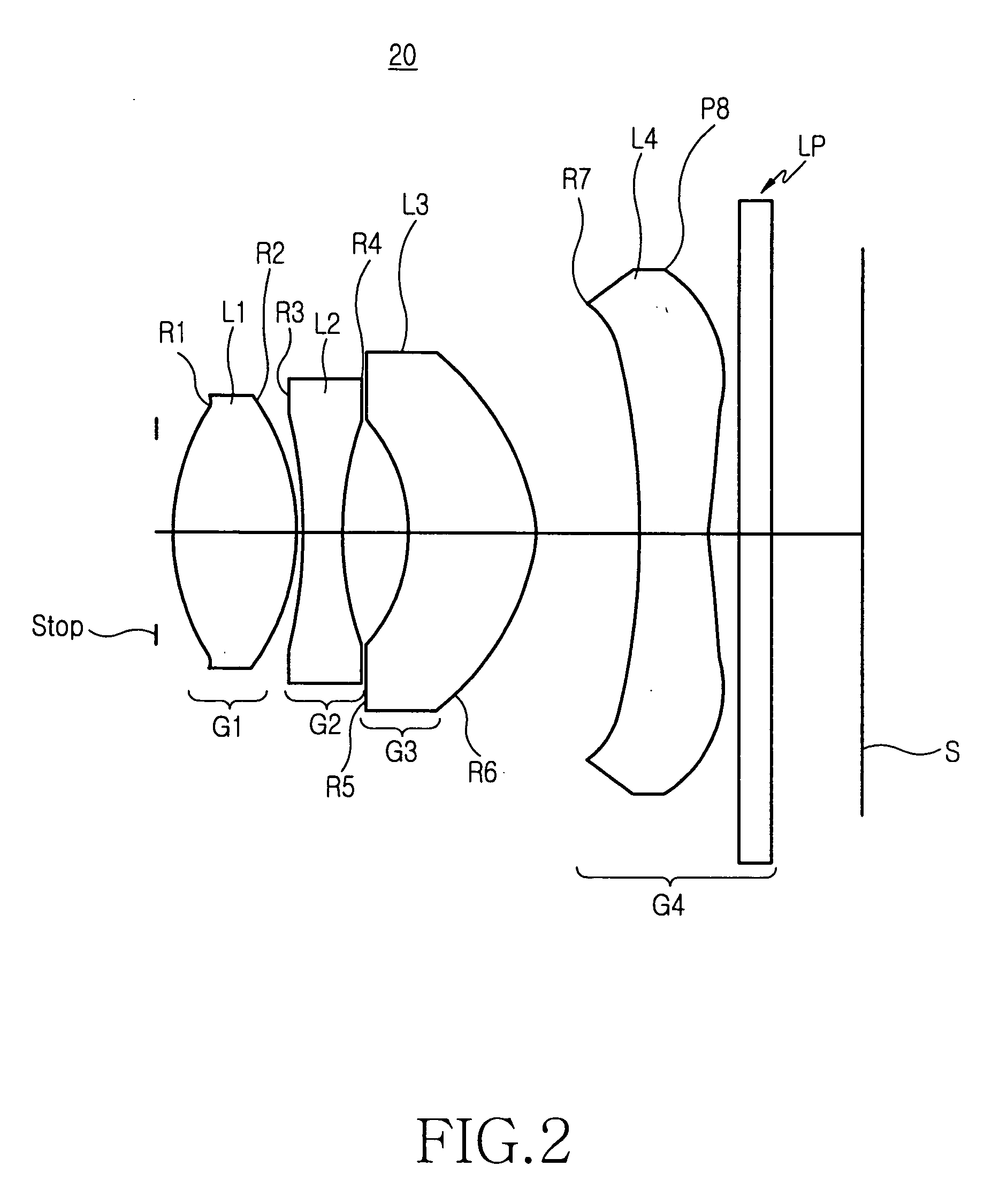
[0046] The optical imaging system 20 according to the second embodiment includes a first lens group G1 having a positive refractive power, a second lens group G2 having a negative refractive power, a third lens group G3 having a positive or negative refractive power, a fourth lens group G4 having a positive or negative refractive power, a stop, and a thin film filter or an optical filter (LP).
[0047] The first lens group G1 includes a first lens L1, both surfaces R1 and R2 of which are aspheric. The thickness of the first lens L1 is 1.174399 mm. The first lens L1 is separated from the stop by 0.158423 mm.
[0048] The second lens group G2 includes a second lens L2 having a refractive index of 1.7552 and a distribution value of 27.53, and the second lens L2 has fourth and fifth surfaces R3 and R4 which are aspheric. Referring to Table 1, the second lens L2 is separated from the first lens L1 by 0.05 mm, and has a thickness of 0.363658 mm.
[0049] The third lens group G3 includes a third...
embodiment 3
[0052] The optical imaging system 30 according to the third embodiment includes a first lens group G1 having a positive refractive power, a second lens group G2 having a negative refractive power, a third lens group G3 having a positive or negative refractive power, a fourth lens group G4 having a positive or negative refractive power, a stop, and a thin film filter or an optical filter.
[0053] The first lens group G1 includes a first lens L1, both surfaces R1 and R2 of which are aspheric. Referring to Table 1, the thickness of the first lens L1 is 1.10000 mm. The first lens L1 is separated from the stop by 0.18539 mm.
[0054] The second lens group G2 includes a second lens L2 having a refractive index of 1.7552 and a distribution value of 27.53. The second lens L2 has fourth and fifth surfaces R3 and R4 which are aspheric. Referring to Table 1, the second lens L2 is separated from the first lens L1 by 0.103084 mm, and the thickness thereof is 0.671321 mm.
[0055] The third lens group...
PUM
 Abstract
Description
Claims
Application Information