

Processes and systems for laser crystallization processing of film regions on a substrate utilizing a line-type beam, and structures of such film regions
a laser crystallization and processing system technology, applied in the field of films processing, can solve the problems of conventional methods, system using such line-type beams b>200/b> are currently not suitable for quick processing of samples, and achieve the effect of similar performan
- Summary
- Abstract
- Description
- Claims
- Application Information
AI Technical Summary
Benefits of technology
Problems solved by technology
Method used
Image

Examples
Embodiment Construction
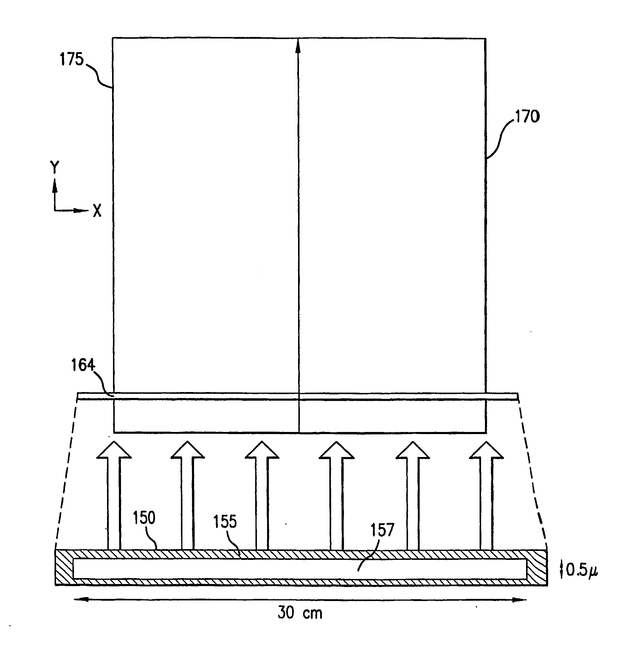
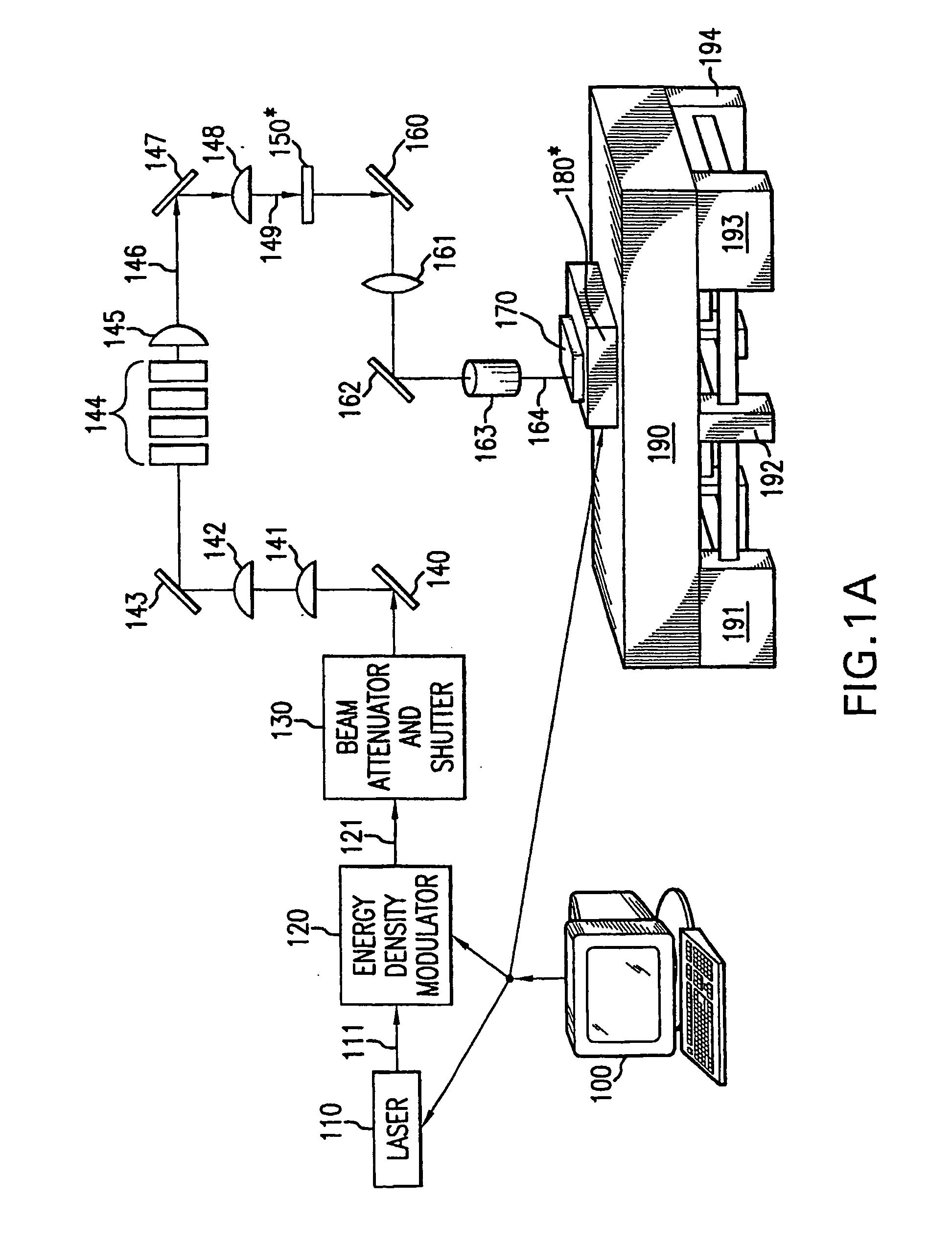
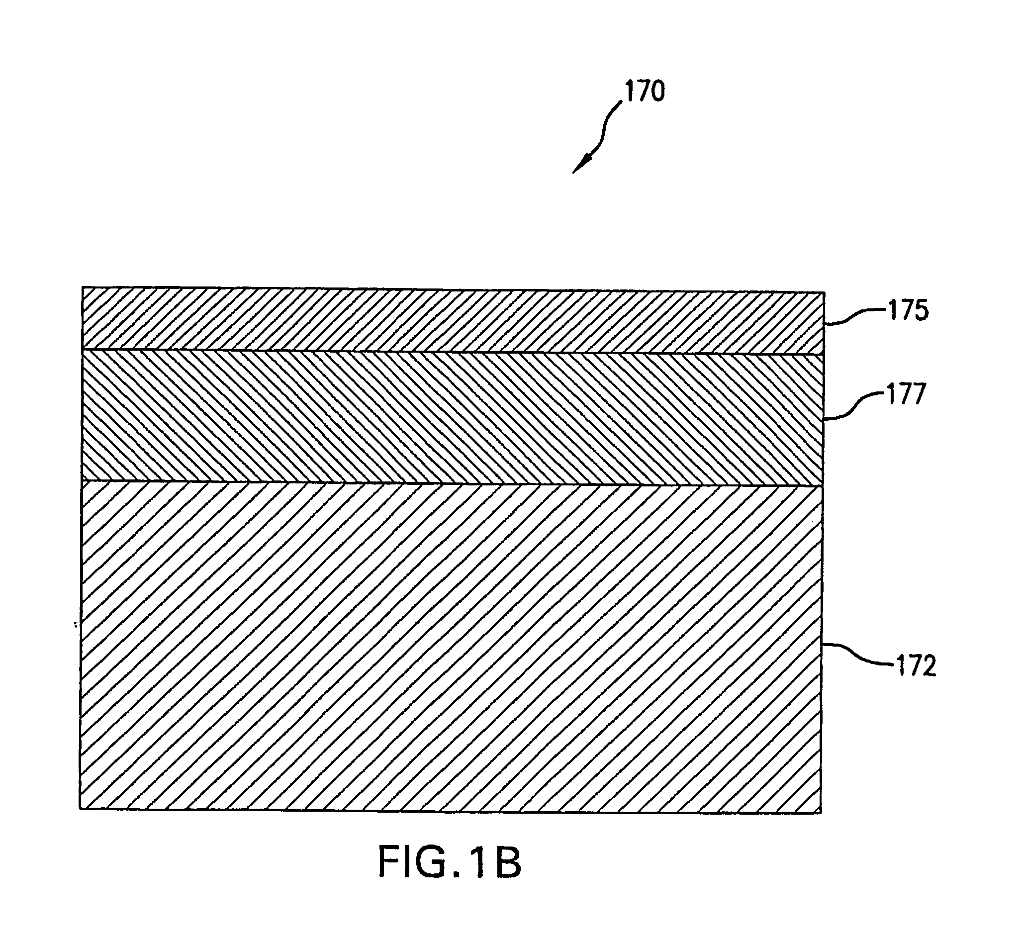
[0028] It should be understood that various systems and methods according to the present invention can be utilized to at least partially melt, then solidify and crystallize one or more areas on a semiconductor thin film (e.g., silicon) using line-type beam pulses, while continuously translating the sample and without re-irradiating the previously irradiated and resolidified areas to generate substantially uniform regions on the thin film. The exemplary embodiments of the systems and process to generate such areas, as well as of the resulting crystallized semiconductor thin films shall be described in further detail below. However, it should be understood that the present invention is in no way limited to the exemplary embodiments of the systems, processes and semiconductor thin films described herein.
[0029] Certain systems for providing a continuous motion SLS are described in U.S. patent application Ser. No. 09 / 526,585 (the “'585 application”), the entire disclosure of which is in...
PUM
 Abstract
Description
Claims
Application Information