
Photovoltaic cells based on nanoscale structures

Active Publication Date: 2007-01-18
BANPIL PHOTONICS
View PDF19 Cites 42 Cited by
  • Summary
  • Abstract
  • Description
  • Claims
  • Application Information

AI Technical Summary

Benefits of technology

[0015] It is also another object of this invention to provide the structures of the photovoltaic cells based on the carbon-nanotubes or semiconductor wires or rods which could provide more junction area per unit physical area, which results in increasing the power generation per unit area over conventional photovoltaic cells.
[0016] This invention offers to generate power 100 times per unit area ad beyond over conventional photovoltaic cells. Also, the proposed photovoltaic cells are highly radiation tolerant, necessary in the space application. The main advantages of these inventions are that today's highly matured semiconductor process technologies can be used to fabricate the photovoltaic cell which has the power generation capability a few order and beyond as compared with that of conventional photovoltaic cell.

Problems solved by technology

Although the fabrication processes of amorphous silicon based photovoltaic cells are rather simple and inexpensive, one notable downside of this type of cell is its vulnerability to defect-induced degradation that decreases its conversion efficiency.
], which again raise issues associated with toxic natures of these materials.
Synthesis processes of single crystalline group III-V are in general very costly because of substantial complications involved in epitaxial growth of group III-V single crystalline compound semiconductors.
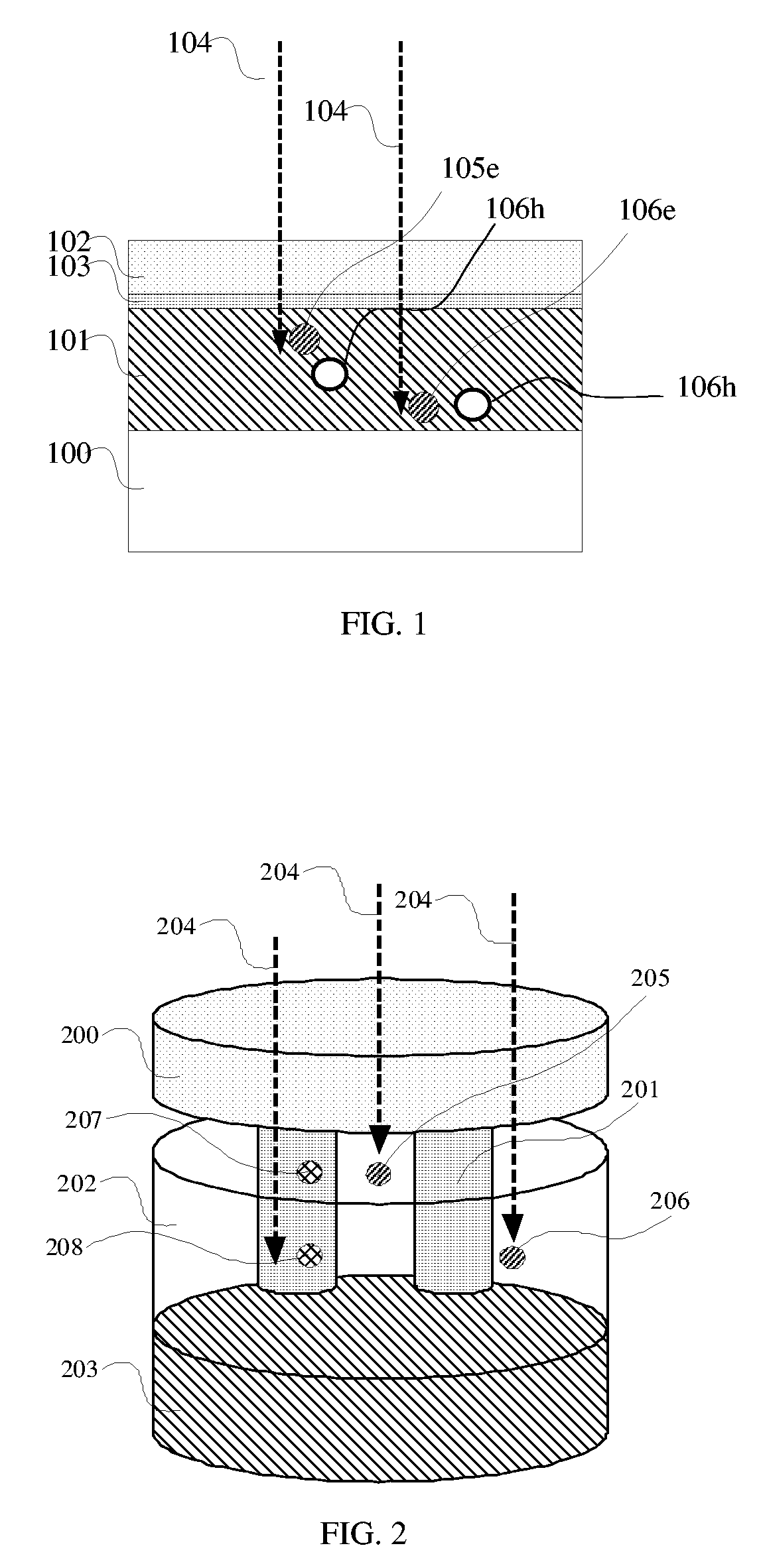
For a monochromatic light, the PCGE of ˜100% can be achieved by simply making the p-type layer 101 thicker, however, electrons 106e generated at the region far away from the pn-junction 103 cannot be collected efficiently due to many adverse recombination processes that prevent photo generated carriers from diffusing into the pn-junction 103, thus the basic structure of current photovoltaic cells has its own limitation on increasing the conversion efficiency.
Besides, today's solar cell material is not highly radiation-tolerant.

Method used


Image

  • Photovoltaic cells based on nanoscale structures
  • Photovoltaic cells based on nanoscale structures
  • Photovoltaic cells based on nanoscale structures

Examples


Embodiment Construction

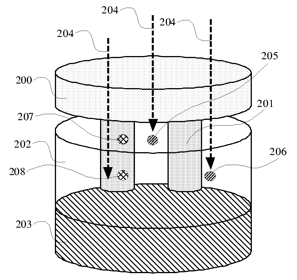
[0027] According to a preferred embodiment illustrated in FIG. 2, shown is a photovoltaic cell comprising plurality of nanometer(s)-scale wires or rods 201 electrically connected to an electrode 200. The nanometer(s)-scale wires or rods 201 can have metallic electrical conduction, p-type or n-type semiconductor electrical conduction. The nanometer(s)-scale wires or rods are further surrounded by an electronic material 202 having metallic electrical conduction, p-type or n-type semiconductor electrical conduction. The electronic material 202 is further electrically connected to an electrode 203. The electrode 200 has direct electrical contact to neither the electrical material 202 nor the electrode 203. As described above, the electrode 200 is intended to serve as a common electrode that connects all wires or rods 201. The electrode 203 is provided for the electronic material 202. The interface between the nanometer scale wires or rods 201 and the electronic material 202 form pn- or ...


PUM


Abstract

Novel structures of photovoltaic cells (also treated as solar cells) are provided. The Cells are based on the nanometer-scaled wire, tubes, and / or rods, which are made of the electronics materials covering semiconductors, insulator or metallic in structure. These photovoltaic cells have large power generation capability per unit physical area over the conventional cells. These cells can have also high radiation tolerant capability. These cells will have enormous applications such as in space, in commercial, residential and industrial applications.

Description

CROSS REFERENCE TO RELATED APPLICATIONS [0001] This application claims the benefit of U.S. Provisional Patent Application No. 60 / 522,134 filed on Aug. 19, 2004.FIELD OF INVENTIONS [0002] This patent specification relates to structures of photovoltaic cells (also solar cells). More specifically, it relates to structures of photovoltaic cells comprising numerous nanometer-scale wires, rods and / or tubes to have large power generation capability per unit area. The photovoltaic cells have also highly radiant tolerant, necessary for space applications. These photovoltaic cells can be used in commercial, residential, and also industrial application for power generation. BACKGROUND OF THE INVENTIONS [0003] Photovoltaic cells where light is converted into electric power to be fed to external loads electrically connected to the photovoltaic cells have been prevailing in a wide range of application fields such as consumer electronics, industrial electronics and space exploration. In consumer e...

Claims


Application Information

Patent Timeline
IPC IPC(8): H01L31/00
CPCH01L31/0352H01L31/03529Y02E10/50H01L31/04H01L31/07H01L31/036
Inventor KOBAYASHI, NOBUHIKO P.DUTTA, ACHYUT K.
Owner BANPIL PHOTONICS
Learn More