El functional film el element

Inactive Publication Date: 2007-01-18
IFIRE IP CORP
View PDF10 Cites 17 Cited by
  • Summary
  • Abstract
  • Description
  • Claims
  • Application Information

AI Technical Summary

Benefits of technology

[0012] Recently, there has been a demand for displays with still higher brightness, high contrast, high detail, low power consumption and reliability. However, even in the case of an inorganic EL element comprising a light-emitting body having the aforesaid 5-layer structure of the prior

Problems solved by technology

However, even in the case of an inorganic EL element comprising a light-emitting body hav

Method used


Image

  • El functional film el element
  • El functional film el element
  • El functional film el element

Examples


example 1

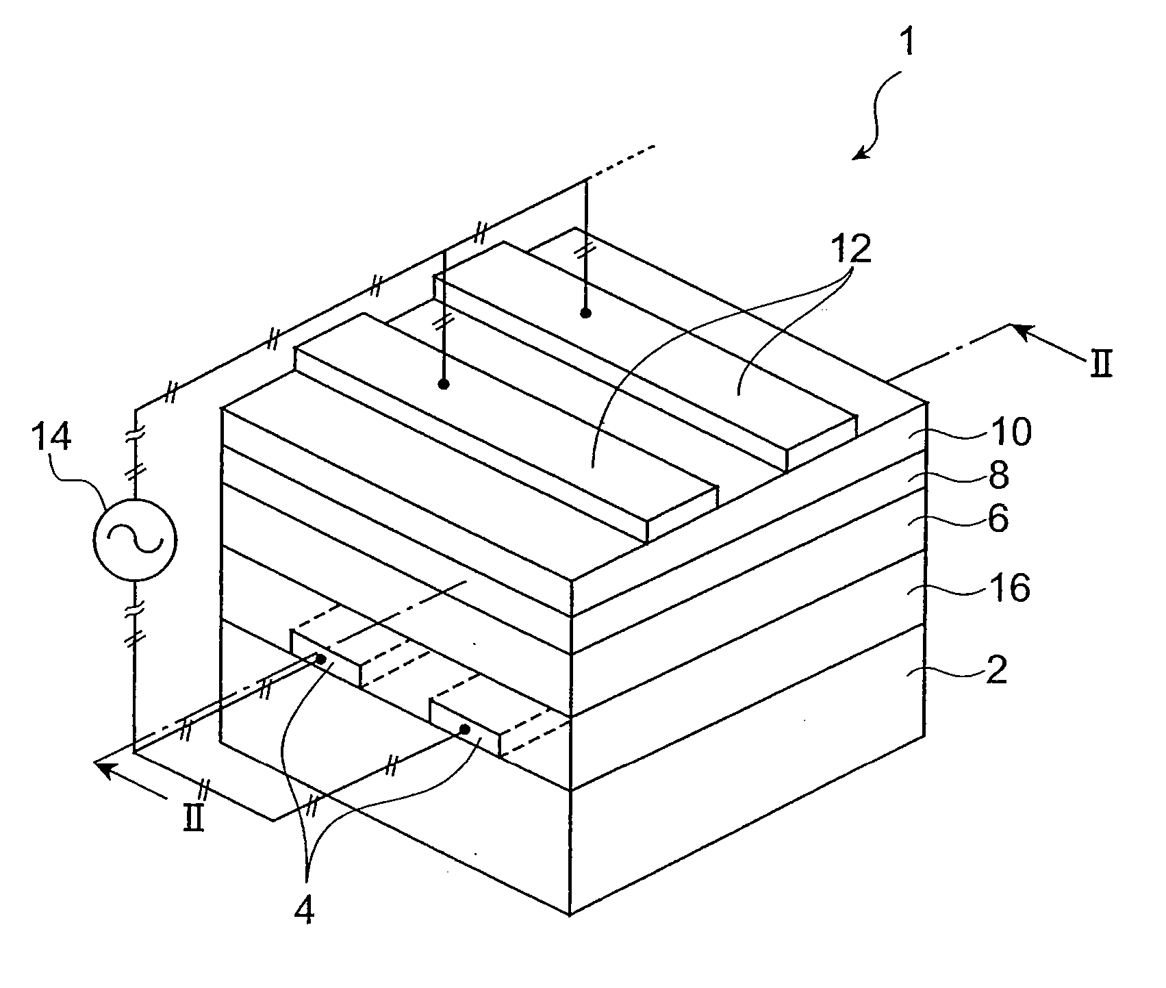
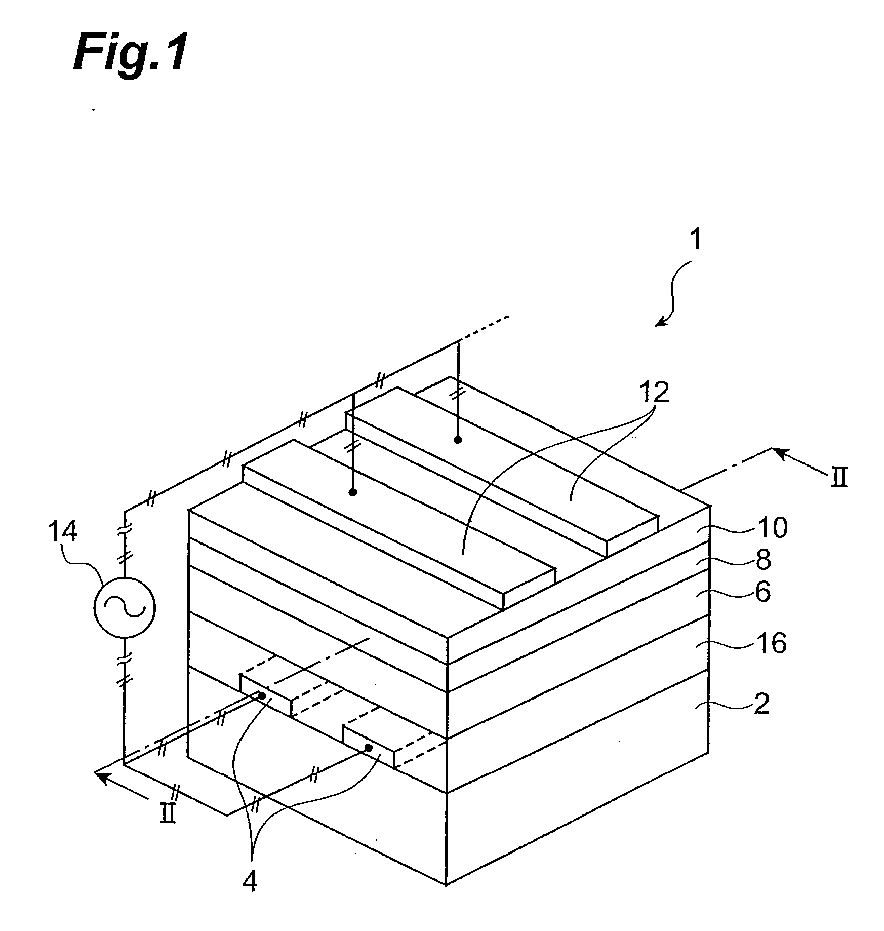
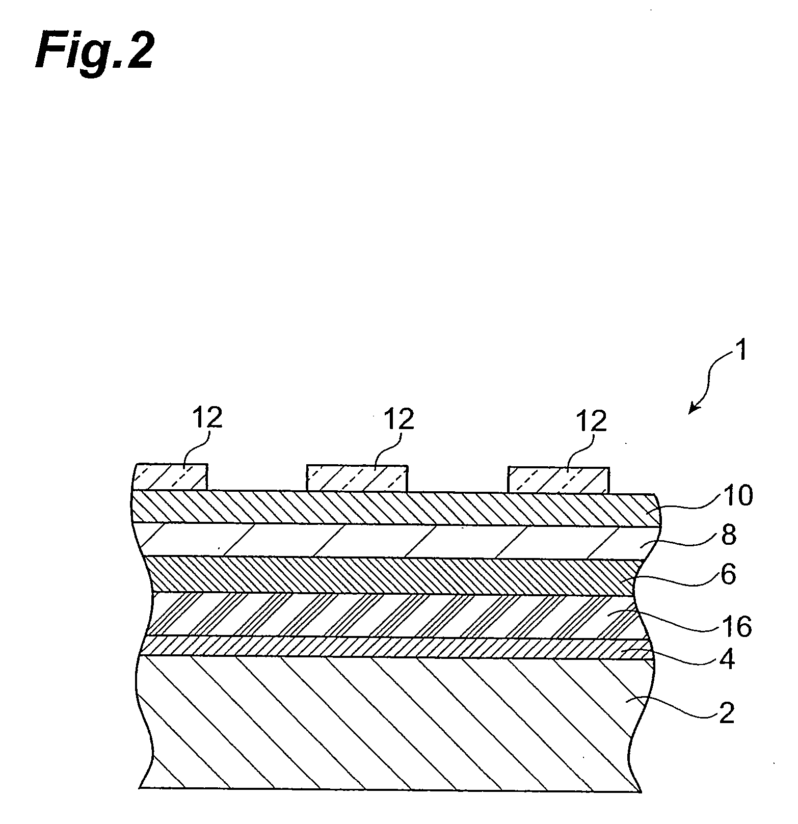
[0073] First, Al2O3as a substrate material was machined into a sheet shape to give a substrate 2. Next, after screen-stenciling an Au powder metal paste on this substrate 2, it was calcinated to form a lower electrode 4. Next, using PMN-PT(Pb(Mg1 / 3Nb2 / 3)O3-PbTiO3) as a thick film insulator layer material, this was formed into a powder, a binder, dispersant and solvent were added to form a thick film paste which was applied to the substrate 2 on which the lower electrode 4 was formed, dried, and calcinated to form a thick film insulator layer 16.

[0074] Next, after forming the EL functional layer 6 of Al2O3on the thick film insulator layer 16 by vapor deposition using Al2O3pellets, another carrier doping layer of ZnS was formed thereupon by vapor deposition using ZnS pellets. Further, the laminate was placed in a chamber containing an EB (electron beam) source into which Ga2O3 pellets were introduced, and an EB source into which MgO pellets with 15 mol % added Eu were introduced.

[00...

example 2

[0078] Plural EL elements according to the invention were obtained as in the first example, except that the EL functional layers 6, 10 were layers of Ga2O3 as described below, and the other carrier doping layer of ZnS was not provided.

[0079] Specifically, while introducing O2 gas (flow rate 10 sccm) into a chamber with an EB source into which Ga2O3 pellets had been introduced, a reactive gas starting material was vaporized from the EB source, and while rotating the laminate (laminate after forming the thick film insulator layer 16 or laminate after forming the light-emitting layer 8) heated to 150° C., the functional layers 6, 10 comprising Ga2O3 were formed on the thick film insulator layer 16 or the light-emitting layer 8.

example 3

[0080] Plural EL elements were obtained as in Example 2, except that the EL functional layers 6, 10 were layers of Ga2O3:Eu as described below.

[0081] Specifically, while introducing O2 gas (flow rate 10 sccm) into a chamber with an EB source into which Ga2O3 pellets had been introduced, and an EB source into which Eu2O3 pellets had been introduced, reactive gas starting materials were simultaneously vaporized from the EB sources, and while rotating the laminate (laminate after forming the thick film insulator layer 16 or laminate after forming the light-emitting layer 8) heated to 150° C., the EL functional layers 6, 10 were formed on the thick film insulator layer 16 or the light-emitting layer 8.

[Measurement of Light-Emitting Voltage and Relative Brightness]

[0082] As test sample (1), among the EL elements of Example 1, an element was selected wherein the thicknesses of the EL functional layers 6, 10 of Al2O3 were 30 and 70 nm, respectively, the thickness of the other carrier do...


PUM


Abstract

An EL element 1 comprises EL functional layers 6, 10 comprising Ga2O3:Eu between a thick film insulator layer 16 and an upper electrode 12 provided on a substrate 2 on which a lower electrode 4 was formed and a light-emitting layer 8 comprising MgGa2O4 formed therebetween. The EL functional layers 6, 10 have the dual functions of insulating layers and electron doping layers. Due to this, the EL element 1 has a low drive voltage and high light-emitting brightness, and the structure of the EL element is simplified.

Description

TECHNICAL FIELD [0001] The present invention relates to an EL functional film and an EL element. BACKGROUND ART [0002] Electroluminescence (in the invention, “EL”) elements may be broadly divided into inorganic EL elements and organic EL elements according to the difference of component materials of the light-emitting body. Inorganic EL elements which use inorganic materials for the light-emitting body have the characteristic of a long light-emission life as compared with organic EL elements which use organic materials for the light-emitting body, and are mainly used in applications requiring high durability, such as the backlight of a clock, LCD (liquid crystal display) or in-vehicle monitor. [0003]FIG. 3 is a perspective view showing the principal parts of the typical construction of a prior art inorganic EL element. An EL element 20 is a double insulation type thin film EL element, wherein stripe-like lower electrodes 22, lower insulator layer 24, light-emitting layer 26, upper i...

Claims


Application Information

Patent Timeline
IPC IPC(8): H05B33/14H01J1/62C09K11/00C09K11/56C09K11/62C09K11/64C09K11/77H01L51/50H05B33/22
CPCC09K11/7729C09K11/621H05B33/22
Inventor TAKAHASHI, MASAKIYANO, YOSHIHIKOOIKE, TOMOYUKIKATAOKA, NARUKI
Owner IFIRE IP CORP
Why Eureka
Try Eureka