
Voltage-controlled oscillator circuit and PLL circuit

a voltage control and oscillator circuit technology, applied in pulse automatic control, pulse generation by logic circuits, pulse techniques, etc., can solve the problems of increasing increasing noise sources, and limiting improvements of jitter performance, so as to reduce noise sources, increase circuit scale and power consumption, and limit the effect of improving jitter performan

Inactive Publication Date: 2007-01-25
SONY CORP
View PDF3 Cites 1 Cited by
  • Summary
  • Abstract
  • Description
  • Claims
  • Application Information

AI Technical Summary

Benefits of technology

[0043] However, this method has a problem of increases in circuit scale and power consumption because separate circuits such as the replica cell, the operational amplifier and the like are added. In addition, the addition of the separate circuits increases noise sources, and limits improvements of jitter performance.
[0044] The present invention has been made in view of the above. It is accordingly desirable to provide a voltage-controlled oscillator and a PLL circuit that suppress distortion of an oscillation waveform of a ring VCO and improve phase noise and jitter performance with a simple constitution.
[0046] Such an oscillator circuit cancels out the vibrations of the nodes of the VCO cells by the vibration canceling section. It is thereby possible to suppress and reduce distortion of the differential signals output from the VCO cells, and phase noise and jitter.
[0047] According to the present invention, the vibration at each node is suppressed and reduced by canceling out the vibrations of the nodes of the VCO cells by the vibration canceling section. It is thereby possible to easily and reliably prevent unnecessary vibration or distortion caused by operation of the switching elements in a triode region. Thus, it is possible to reduce distortion of an oscillation waveform, and improve phase noise and jitter performance.

Problems solved by technology

However, this method has a problem of increases in circuit scale and power consumption because separate circuits such as the replica cell, the operational amplifier and the like are added.
In addition, the addition of the separate circuits increases noise sources, and limits improvements of jitter performance.

Method used


Image

  • Voltage-controlled oscillator circuit and PLL circuit
  • Voltage-controlled oscillator circuit and PLL circuit
  • Voltage-controlled oscillator circuit and PLL circuit

Examples


first embodiment

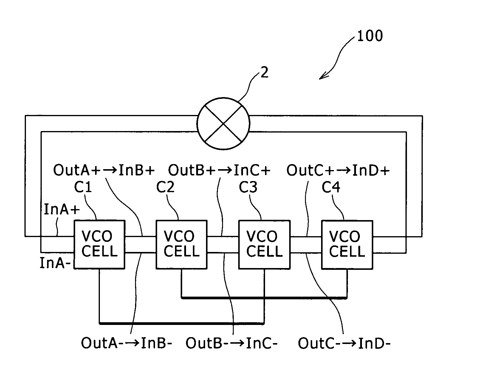
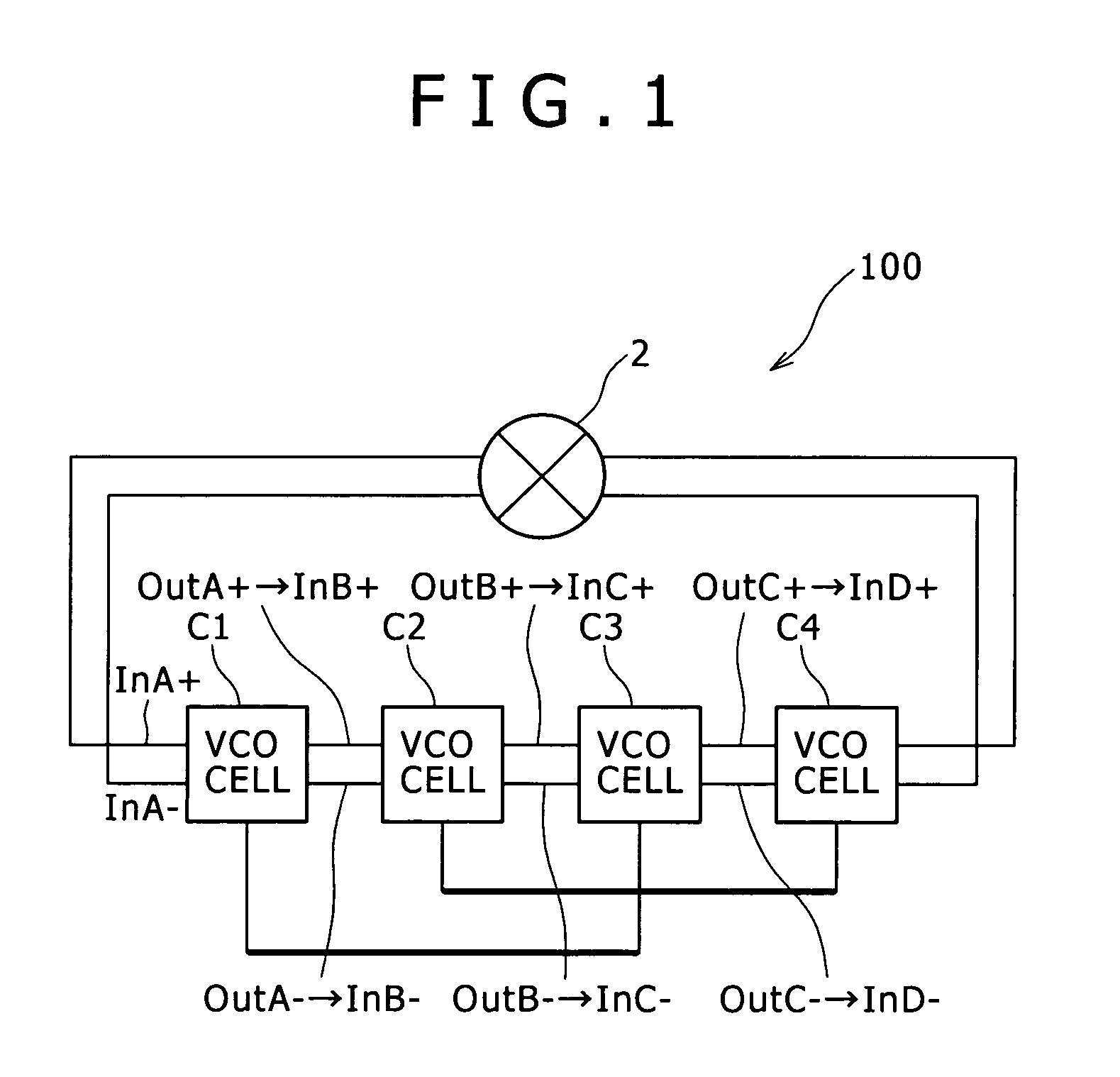
[0066]FIG. 1 is a block diagram of assistance in explaining an oscillator circuit according to a

[0067] An oscillator circuit 100 is a voltage-controlled oscillator (VCO). The oscillator circuit 100 changes the frequency of an oscillating signal according to a control voltage signal corresponding to a phase difference between a reference signal and a feedback signal.

[0068] The oscillator circuit 100 includes four VCO cells C1 to C4 having a same internal configuration, and an inverting unit 2 for inverting differential signal lines connected to the VCO cell C1 and the VCO cell C4.

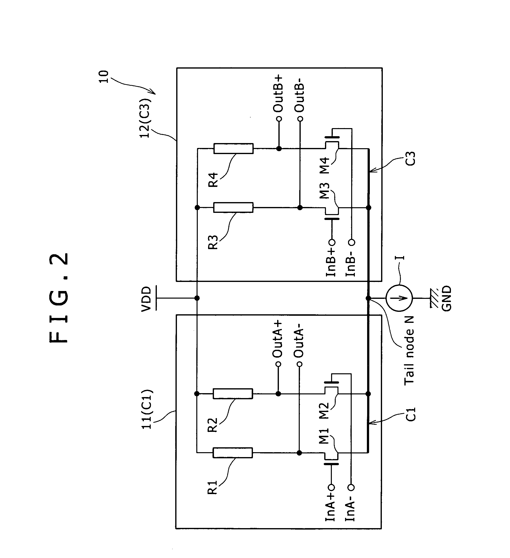
[0069] The tail nodes (to be described later) of the VCO cell C1 and the VCO cell C3 are connected to each other. The tail nodes of the VCO cell C2 and the VCO cell C4 are connected to each other.

[0070] The VCO cells C1 to C4 are cascaded in a plurality of stages in the form of a ring. The output terminals of the VCO cell C1 are connected to the input terminals of the VCO cell C2. The output terminals of ...

second embodiment

[0100] an oscillator circuit will next be described.

[0101] Description in the following will be made of oscillator circuits 100b and 100c according to the second embodiment, centering on differences from the foregoing first embodiment, and description of similar items will be omitted.

[0102]FIG. 6 is a block diagram showing an oscillator circuit according to the second embodiment.

[0103] The oscillator circuit 100b according to the second embodiment is different from the oscillator circuit 100 according to the first embodiment in terms of combinations of VCO cells having tail nodes connected to each other.

[0104] The oscillator circuit 100b has VCO cells C1, C2, C3, C4, C5, and C6.

[0105] Letting N be the number of VCO cells (N is an even number of more than one), in the oscillator circuit 100b, the tail nodes of two VCO cells at an interval of N / 2 stages are connected to each other. Specifically, the tail nodes of the VCO cell C1 and the VCO cell C4 are connected to each other; the...

third embodiment

[0110] an oscillator circuit will next be described.

[0111] Description in the following will be made of an oscillator circuit 100d according to the third embodiment, centering on differences from the foregoing first embodiment, and description of similar items will be omitted.

[0112]FIG. 8 is a block diagram showing the oscillator circuit according to the third embodiment.

[0113] The oscillator circuit 100d according to the third embodiment is different from the oscillator circuit 100 according to the first embodiment and the oscillator circuit 100b according to the second embodiment in that the oscillator circuit 100d according to the third embodiment uses VCOs in an odd number of stages (an odd number of VCOs).

[0114] The oscillator circuit 100d includes: VCO cells C1, C2, and C3; a capacitance Ca1 disposed between the tail nodes of the VCO cells C1 and C2; a capacitance Ca2 disposed between the tail nodes of the VCO cells C2 and C3; and a capacitance Ca3 disposed between the tail...


PUM


Abstract

A differential type voltage-controlled oscillator circuit including: a plurality of VCO cells each having one pair of switching elements, the switching elements having one terminal side connected to a voltage source via a load and another terminal side connected to a common current source via a common node, the switching elements being supplied with differential signals, the plurality of VCO cells outputting differential signals different in phase from the differential signals; and a vibration canceling section connecting the plurality of VCO cells such that vibration at each node is cancelled.

Description

CROSS REFERENCES TO RELATED APPLICATIONS [0001] The present invention contains subject matter related to Japanese Patent Application JP 2005-202913 filed with the Japanese Patent Office on Jul. 12, 2005, the entire contents of which being incorporated herein by reference. BACKGROUND OF THE INVENTION [0002] 1. Field of the Invention [0003] The present invention relates to a voltage-controlled oscillator circuit and a PLL circuit, and particularly to a differential type voltage-controlled oscillator circuit and a PLL circuit including the same. [0004] 2. Description of the Related Art [0005] In radio communications using portable telephones and the like, serial communications through various cables, systems for reproducing digitally recorded data from disk media (read channels), and the like, a PLL (Phase-Locked Loop) circuit is widely used to generate an oscillating signal with a high spectrum precision and generate a clock signal locked in frequency and phase to a data signal. [0006...

Claims


Application Information

Patent Timeline
IPC IPC(8): H03K3/03
CPCH03B27/00H03K3/013H03L7/193H03L7/0995H03K3/0322H03K3/354H03L7/099
Inventor UENO, YOSUKE
Owner SONY CORP
Learn More