

Transistor
a transistor and transistor technology, applied in the field of transistors, can solve the problems of reducing the performance of the mos transistor, the parasitic resistance of the ldd and mdd regions, and the large limitation of the improvement of the transistor performance,
- Summary
- Abstract
- Description
- Claims
- Application Information
AI Technical Summary
Benefits of technology
Problems solved by technology
Method used
Image

Examples
Embodiment Construction
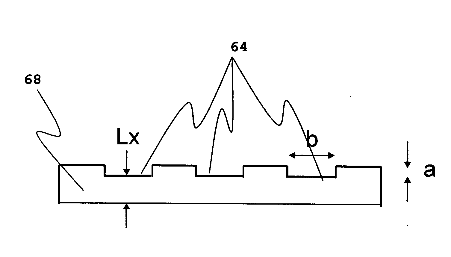
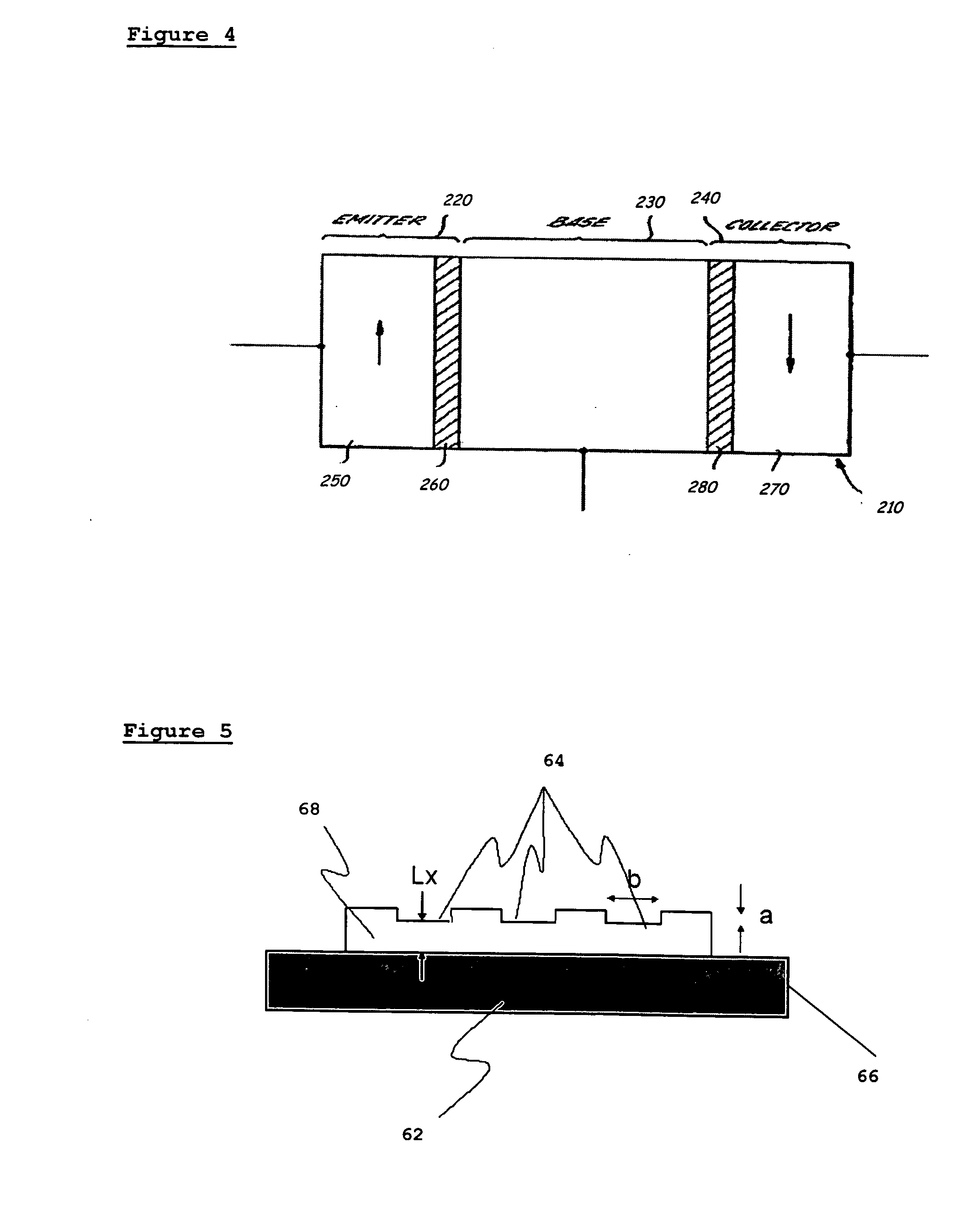
[0020] Referring now to FIG. 6, which shows a modified gate structure 68 of the present invention, having indents 64 along one side of said gate structure. Preferably said one or more indents have a depth approximately 5 to 20 times a roughness of the surface into which they indent, and a width approximately 5 to 15 times the depth. Preferably the walls of the indents are substantially perpendicular to one another, and the edges of the indents are substantially sharp. Typically the depth of the indents a is ≧λ / 2, wherein λ is the de Broglie wavelength, and the depth is greater than the surface roughness of the metal surface. Typically the width b of the indents is >>λ, wherein 80 is the de Broglie wavelength. Typically the thickness of the slab Lx is a multiple of the depth, preferably between 5 and 15 times said depth, and preferably in the range 15 to 75 nm.
[0021] The indented gate may resemble a corrugated pattern of squared-off, “u”-shaped ridges and / or valleys. Alternatively, ...
PUM
 Abstract
Description
Claims
Application Information