Wiring substrate, electro-optic device, electric apparatus, method of manufacturing wiring substrate, method of manufacturing electro-optic device, and method of manufacturing electric apparatus

a technology of wiring substrate and electrooptic device, which is applied in the direction of semiconductor device details, semiconductor/solid-state device details, instruments, etc., can solve the problems of requiring complicated processes, in general, and achieve the improvement of insulating performance, insulating performance between the substrate and the first film, and insulating performan

Inactive Publication Date: 2007-02-01
SEIKO EPSON CORP
View PDF8 Cites 7 Cited by
  • Summary
  • Abstract
  • Description
  • Claims
  • Application Information

AI Technical Summary

Benefits of technology

[0007] In view of the technical problem, an advantage of the invention is to improve insulating performance between films formed on a wiring substrate having a multi layer wiring structure without complicating the manufacturing process.
[0008] A wiring substrate according to an aspect of the invention includes a substrate, a first film, and a second film formed between the substrate and the first film, and an empty space is formed between at least a part of the second film and the substrate.
[0009] Further, in the wiring substrate according to the aspect of the invention, at least a part of the second film has contact with the substrate, and a part of the first film positions above the empty space. Further, the second film preferably includes an insulating material. Thus, the insulating performance between the substrate and the first film can be improved.
[0010] Further, in the wiring substrate described above, the first film can include a semiconductor material, a gate insulating film can be formed on the first film, and a gate electrode can be formed on the gate insulating film. Thus, the insulating performance between the substrate and the semiconductor film can be improved in a so-called top gate type transistor.
[0011] Further, in the wiring substrate described above, the first film can include a first conductive material. Note here that the conductive material includes a metallic material and a conductive organic material. For example, by forming the gate electrode with the first film, it can be applied to a so-called bottom gate type transistor.
[0012] Further, in the wiring substrate described above, the substrate can have a third film including a second conductive material, and at least a part of the second film and at least a part of the empty space can be formed above the third film. Thus, assuming that the first film and the third film are wiring patterns, for example, the insulating performance between the both wiring patterns can be improved.

Problems solved by technology

However, the technology for forming a hollow area between films as, for example, the SON in the past, is apt to require complicated process, in general.

Method used


Image

  • Wiring substrate, electro-optic device, electric apparatus, method of manufacturing wiring substrate, method of manufacturing electro-optic device, and method of manufacturing electric apparatus
  • Wiring substrate, electro-optic device, electric apparatus, method of manufacturing wiring substrate, method of manufacturing electro-optic device, and method of manufacturing electric apparatus
  • Wiring substrate, electro-optic device, electric apparatus, method of manufacturing wiring substrate, method of manufacturing electro-optic device, and method of manufacturing electric apparatus

Examples


first embodiment

[0036] First Embodiment

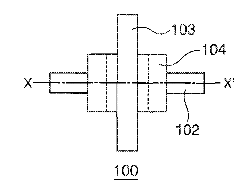
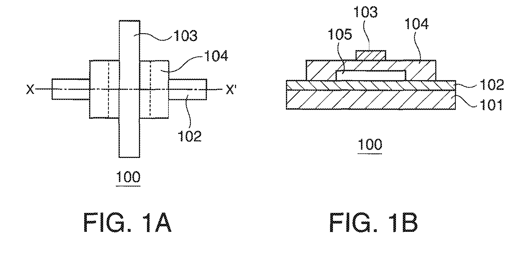
[0037]FIGS. 1A and 1B are views schematically showing the structure of a wiring substrate 100 according to a first embodiment of the invention. FIG. 1A is a top view of the wiring substrate 100, and FIG. 1B is a cross-sectional view along the X-X′ line in FIG. 1A. The wiring substrate 100 is provided with a substrate (base body) 101, first wiring (a third film) 102, a second wiring (a first film) 1 (03, an insulating film (a second film) 104 formed between the first wiring 102 and the second wiring 103. The insulating film 104 has a hollow section, namely an empty space 105 is formed between the first wiring 102 and the insulating film 104.

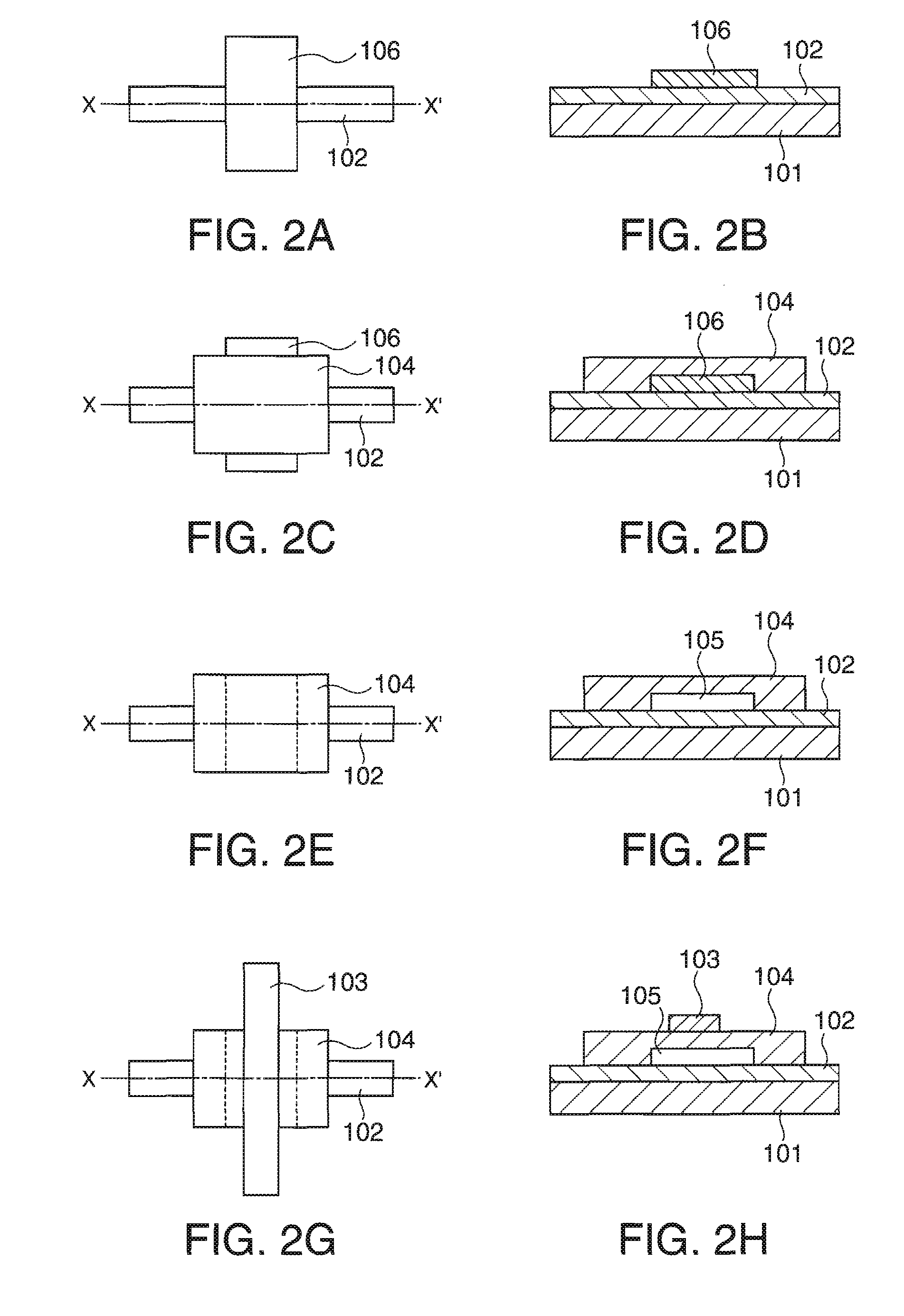
[0038] Then, a manufacturing process of the wiring substrate 100 will be explained with reference to FIGS. 2A through 2H. FIGS. 2A, 2C, 2E and 2G are top views of the wiring substrate 100, and FIGS. 2B, 2D, 2F and 2H are cross-sectional views along the respective X-X′ lines in FIGS. 2A, 2C, 2E and 2G.

[0039] Firstly, as sho...

second embodiment

[0045] Second Embodiment

[0046]FIGS. 4A through 4C are views schematically showing the structure of a wiring substrate 110 according to a second embodiment of the invention. FIG. 4A is a top view of the wiring substrate 110. FIG. 4B is a cross-sectional view along the Y1-Y1′ line in FIG. 4A. FIG. 4C is a cross-sectional view along the Y2-Y2′ line in FIG. 4A. The difference from the FIGS. 1A and 1B is that the second wiring 103 is formed with a greater width than the width of the empty space 105.

[0047] The overlapping section of the first wiring 102 with the second wiring 103 is isolated with the double layer structure composed of the insulating film 104 and the empty space 105 in the wiring substrate 100 shown in FIGS. 1A and 1B. In contrast in the wiring substrate 110, there are two sections, namely a section where the first wiring 102 and the second wiring 103 are isolated from each other with the double layer structure of the insulating film 104 and the empty space 105 as shown i...

third embodiment

[0049] Third Embodiment

[0050]FIGS. 5A through 5C are views schematically showing the structure of a wiring substrate 120 according to a third embodiment of the invention. FIG. 5A is a top view of the wiring substrate 120. FIG. 5B is a cross-sectional view along the X-X′ line in FIG. 5A. FIG. 5C is a cross-sectional view along the Y-Y′ line in FIG. 5A. The difference from one shown in FIGS. 1A and 1B is a direction in which the empty space 105 is formed.

[0051] Although in the embodiment shown in FIGS. 1A and 1B, the empty space 105 is provided along the direction in which the second wiring 103 extends, in the wiring substrate 120 the empty space 105 is provided in a direction perpendicular to the direction in which the second wiring 103 extends as shown in FIGS. 5A through 5C. Since the second wiring 103 does not cross the opening sections in the both ends of the insulating film 104, namely the both ends of the empty space 105, the broken line in the second wiring 103 becomes hard t...


PUM


Abstract

A wiring substrate includes a substrate, a first film, and a second film formed between the substrate and the first film, and an empty space is formed between at least a part of the second film and the substrate.

Description

BACKGROUND OF THE INVENTION [0001] 1. Technical Field [0002] The present invention relates to a wiring substrate, an electro-optic device, an electric apparatus, a method of manufacturing a wiring substrate, a method of manufacturing an electro-optic device, and a method of manufacturing an electric apparatus. [0003] 2. Related Art [0004] In a wiring substrate of a semiconductor device having a multilayer wiring structure or the like, conductors or a semiconductor and a conductor need to be isolated from each other in areas where they overlap. As a method of isolation, a method of providing an insulating film with low permittivity or a method of forming an empty space (SON: Silicon on Nothing) is known. In particular, the empty space can increase the insulation performance. [0005] A technology for utilizing the empty space as the isolation area with low permittivity is described in, for example, JP-A-2001-144276 or JP-A-2001-217312. [0006] However, the technology for forming a hollo...

Claims


Application Information

Patent Timeline
Patent Type & Authority Applications(United States)
IPC IPC(8): H01L21/44
CPCG02F1/136286H01L27/14601H01L29/78651H01L29/66742H01L29/78603H01L27/14692H01L21/18H01L21/31H01L21/3205H01L21/768
Inventor YUDASAKA, ICHIO
Owner SEIKO EPSON CORP
Why Eureka
Try Eureka