SRAM cell with column select line

a column select line and sram technology, applied in the field of sram array structure, can solve the problems of increasing the difficulty of designing an sram cell, snm degradation, and cells generally suffering from much, so as to minimize data upset and power dissipation, increase read current, and optimize static noise margin

Active Publication Date: 2007-02-01
TEXAS INSTR INC
View PDF10 Cites 27 Cited by
  • Summary
  • Abstract
  • Description
  • Claims
  • Application Information

AI Technical Summary

Benefits of technology

[0012] The following presents a simplified summary in order to provide a basic understanding of one or more aspects of the invention. This summary is not an extensive overview of the invention, and is neither intended to identify key or critical elements of the invention, nor to delineate the scope thereof. Rather, the primary purpose of the summary is to present some concepts of the invention in a simplified form as a prelude to the more detailed description that is presented later. The invention relates to an array structure of SRAM cells (e.g., 6T single ended or 8T differential cells) and method is discussed having variable high and low voltage power supplies to provide to selected columns of the array (or the entire array) a write bias condition during a write operation and a read bias condition during a read operation, wherein the read bias condition is different from the write bias condition. Optimum static noise margin is provided while minimizing data upsets and power dissipation during read and write operations, by allowing the array supply voltage to be kept low during all but the read operation and then, enabled by a column select, only raising the supply to the selected columns for increased read current. In addition, by avoiding boosting the array supply and wordline voltages during write operations, the present invention also minimizes dielectric reliability issues.

Problems solved by technology

As transistor scaling trends continue, however, it becomes increasingly difficult to design an SRAM cell that has both adequate static noise margin (SNM), adequate trip voltage (Vtrip), and also can endure read and write operations over the desired operating range of temperature, bias conditions, and process variations.
Also, if the load is too weak relative to the drive transistor, SNM is degraded.
Single-sided 4T and 5T SRAM cells (e.g., SS 5T SRAM cells) have also been proposed, but these cells generally suffer from much of the above mentioned compromises including poor data stability, low noise margins, and many other such difficult issues.
With technology scaling to the 45 nm node and beyond, it may no longer be possible to achieve a balance in the relative strengths of the pass gate, drive, and load transistors over the desired range of temperature and bias conditions as well as process variations.
Therefore, it may be desirable to lower the array Vdd to reduce power dissipation, but low Vdd reduces the stability of the standard 6T SRAM cells.
Similarly, it may be desirable to raise the wordline voltage to improve the SNM margin during write operations; however, the higher wordline voltage may also reduce the stability of the unaddressed cells.
Thus, the current balance in cell design values often involves a trade-off that may translate to a higher incidence of data upsets and / or slower access times during cell read and write operations.
In addition, although a relatively small subset of the cells may be addressed at any one time in the standard memory configuration, power is consumed on all cells of the array.

Method used


Image

  • SRAM cell with column select line
  • SRAM cell with column select line
  • SRAM cell with column select line

Examples


Embodiment Construction

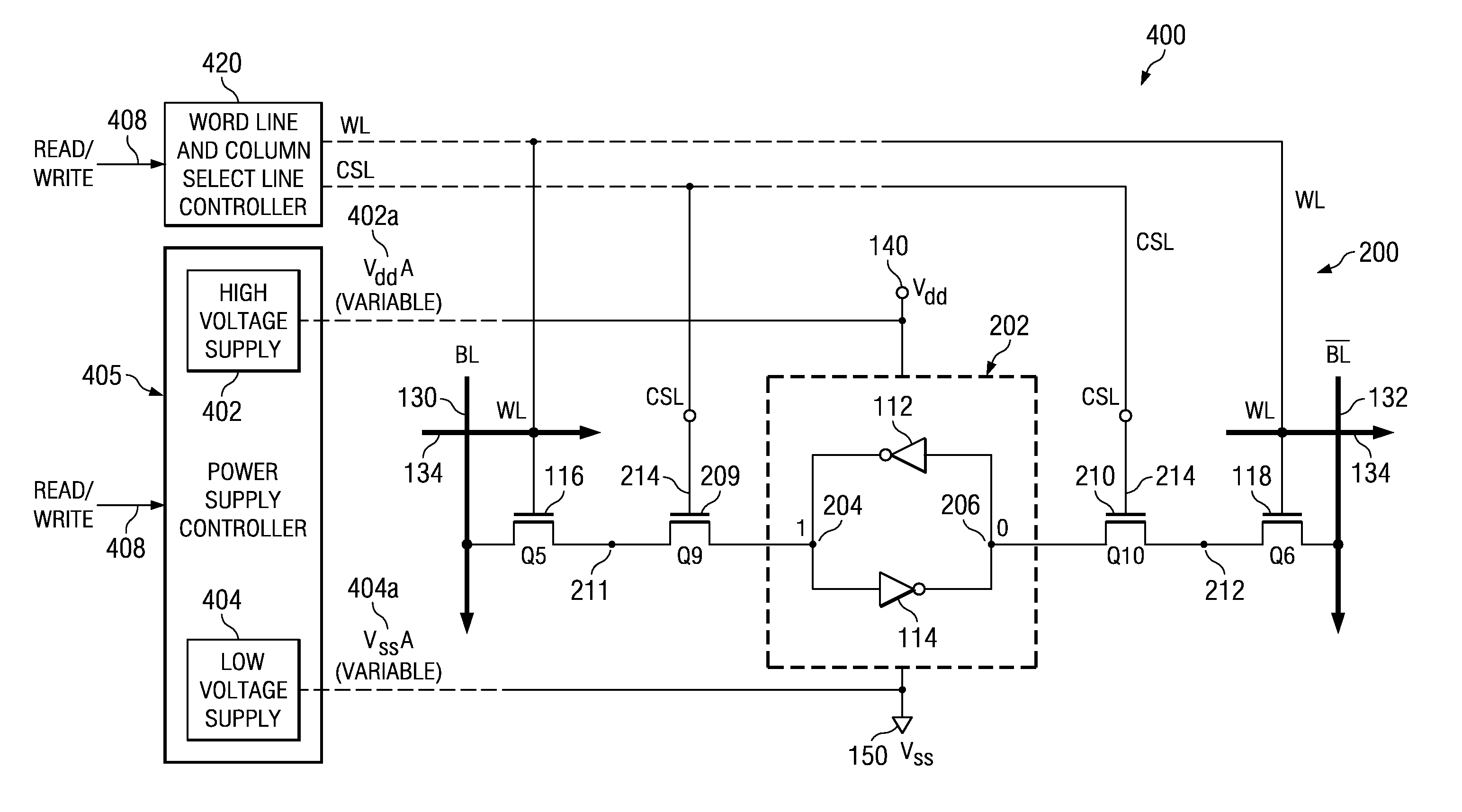
[0042] The present invention will now be described with reference to the attached drawings, wherein like reference numerals are used to refer to like elements throughout. The invention provides an improved SRAM array structure comprising SRAM cells (e.g., single sided 6T or differential 8T cells) having variable high and low voltage power supplies and a method of operating the SRAM array that provides a write bias condition during a write operation and a read bias condition during a read operation, wherein the read bias condition is different from the write bias condition.

[0043] The system and method provides optimum static noise margin while minimizing data upsets and power dissipation during read and write operations, by allowing the array supply voltage to be kept low during all but the read operation and then, enabled by a column select, only raising the supply to the selected columns to provide increased read current. In addition, by avoiding boosting the array supply and word...


PUM


Abstract

An array of SRAM cells (e.g., 6T single-ended or 8T differential cells) and method is discussed having variable high and low voltage power supplies to provide to selected cells of the array a write bias condition during a write operation and a read bias condition to the array during a read operation, wherein the read bias condition is different from the write bias condition.

Description

FIELD OF INVENTION [0001] The present invention relates generally to semiconductor memory devices and more particularly to an improved SRAM array structure and method of operating an SRAM array to improve the static noise margin, and to minimize power dissipation and the risk of destabilizing unaddressed cells of the accessed wordline during write operations in the manufacture of semiconductor products. BACKGROUND OF THE INVENTION [0002] Current trends in the semiconductor and electronics industry require memory devices to be made smaller, faster and require less power consumption. One reason for these trends is that more personal devices are being manufactured that are relatively small and portable, thereby relying on battery power. In addition to being smaller and more portable, personal devices are also requiring increased memory and more computational power and speed. In light of all these trends, there is an ever increasing demand in the industry for smaller, faster, and lower ...

Claims


Application Information

Patent Timeline
Patent Type & Authority Applications(United States)
IPC IPC(8): G11C11/00G11C5/14
CPCG11C11/419G11C11/417
Inventor DENG, XIAOWEIHOUSTON, THEODORE W.
Owner TEXAS INSTR INC
Why Eureka
Try Eureka