Method for forming microlenses of different curvatures and fabricating process of solid-state image sensor

a solid-state image sensor and microlense technology, applied in the field of optical components, can solve the problems of inability to improve the overall sensitivity of the cis device, laborious fabrication, and laborious microlense process, and achieve the effect of saving process time and improving the overall sensitivity of the image sensor

Inactive Publication Date: 2007-02-01
UNITED MICROELECTRONICS CORP
View PDF6 Cites 8 Cited by
  • Summary
  • Abstract
  • Description
  • Claims
  • Application Information

AI Technical Summary

Benefits of technology

[0016] Since the microlenses of different curvatures are form with only one lithography process via the variation of pattern transparencies on a single photomask, much process time is saved as compared with the prior art that forms microlenses of different colors or curvatures with more than one lithography processes. Meanwhile, because the first to third color lights are respectively focused to the first, the second and the third maximal absorption regions, the sensitivities of the image sensor to different color lights are optimized respectively. Hence, the overall sensitivity of the image sensor is improved as compared with the prior art that forms microlenses of different areas or colors.

Problems solved by technology

Therefore, the overall sensitivity of the CIS device cannot be improved.
In addition, forming microlenses of different colors needs more then one lithography processes, so that the fabrication is tedious.
However, this microlens process is very tedious because three lithography processes are conducted to form photoresist islands of three thicknesses for making the three curvatures.

Method used


Image

  • Method for forming microlenses of different curvatures and fabricating process of solid-state image sensor
  • Method for forming microlenses of different curvatures and fabricating process of solid-state image sensor
  • Method for forming microlenses of different curvatures and fabricating process of solid-state image sensor

Examples


Embodiment Construction

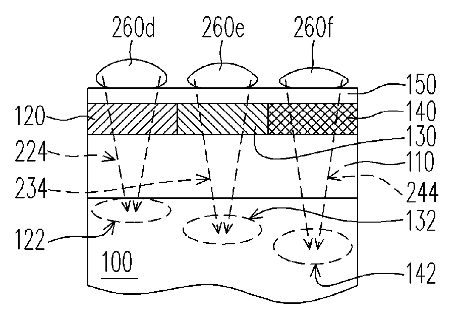
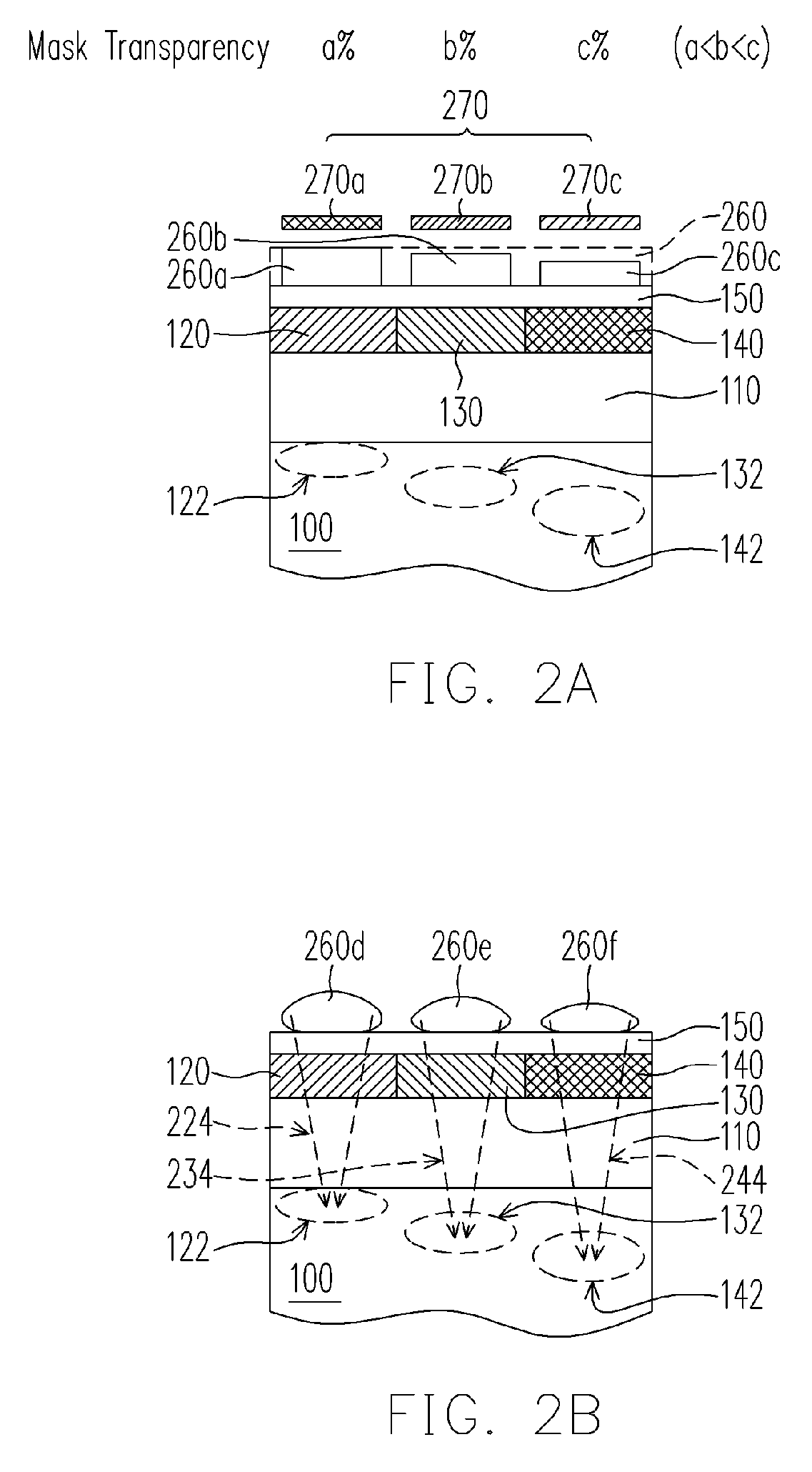
[0021] This invention will be further explained with a fabricating process of a CMOS image sensor as a preferred embodiment, which is illustrated in FIGS. 2A-2B in a cross-sectional view. In this embodiment, the first to third color lights as mentioned above are red light, green light and blue light, respectively, but are not limited to those. The three color lights may alternatively be magenta, cyan and yellow lights, or any other combination of three color lights that can be combined to obtain full colors.

[0022] Referring to FIG. 2A, a semiconductor substrate 100 is provided, having been formed with a circuit (not shown) thereon, which essentially includes CMOS transistors, sensor diodes and necessary interconnect structures, etc. Respective depths D1, D2 and D3 of the maximal absorption regions 142, 132 and 122 of red, green and blue lights in the substrate 100 satisfy the inequality of “D1>D2>D3”.

[0023] Then, a passivation layer 110, such as a thick SiO2 layer, is formed over ...


PUM


Abstract

A method for forming microlenses of different curvatures is described, wherein a transparent photosensitive layer is formed on a substrate having a planar upper surface. A photomask is used to pattern the photosensitive layer, wherein the photomask has at least two patterns of different transparencies thereon such that at least two islands of different thicknesses are defined from the photosensitive layer. Then, the at least two islands are heated and softened to form at least two microlenses of different curvatures.

Description

BACKGROUND OF THE INVENTION [0001] 1. Field of the Invention [0002] The present invention relates to a method for fabricating optical components. More particularly, the present invention relates to a method for forming microlenses of different curvatures, and to a fabricating process of a solid-state image sensor which utilizes the method so that the sensitivities to different color lights can be optimized respectively. [0003] 2. Description of the Related Art [0004] A solid-state image sensor, such as a CCD image sensor or CMOS image sensor (CIS) is essentially composed of red, green and blue pixel sensors that are respectively equipped with red, green and blue filters. To increase the quantum yield of incident light for improving the sensitivity, a microlens can be formed over each color filter to focus the incident light, as described in U.S. Pat. No. 6,379,992, for example. [0005] Referring to FIG. 1A, in a typical microlens process of a CIS device, a substrate 100 is provided, ...

Claims


Application Information

Patent Timeline
Patent Type & Authority Applications(United States)
IPC IPC(8): H01L21/00
CPCG02B3/0012G02B3/0056H01L27/14685H01L27/14621H01L27/14627G02B5/201
Inventor WU, HSIN-PINGLIN, CHIA-HUEI
Owner UNITED MICROELECTRONICS CORP
Why Eureka
Try Eureka