

Semiconductor integrated circuit device and method of fabricating the same
a technology of integrated circuit and semiconductor, applied in the direction of semiconductor devices, basic electric elements, electrical equipment, etc., can solve the problems of gate control function deformation of alignment keys formed on masks, and reduced effective channel length and threshold voltage. , to achieve the effect of stable operation and reduced power consumption
- Summary
- Abstract
- Description
- Claims
- Application Information
AI Technical Summary
Benefits of technology
Problems solved by technology
Method used
Image

Examples
Embodiment Construction
[0023] Advantages and features of the present invention and methods of accomplishing the same may be understood more readily by reference to the following detailed description of preferred embodiments and the accompanying drawings. The present invention may, however, be embodied in many different forms and should not be construed as being limited to the embodiments set forth herein. Rather, these embodiments are provided so that this disclosure will be thorough and complete and will fully convey the concept of the invention to those skilled in the art. Like reference numerals refer to like elements throughout the specification.
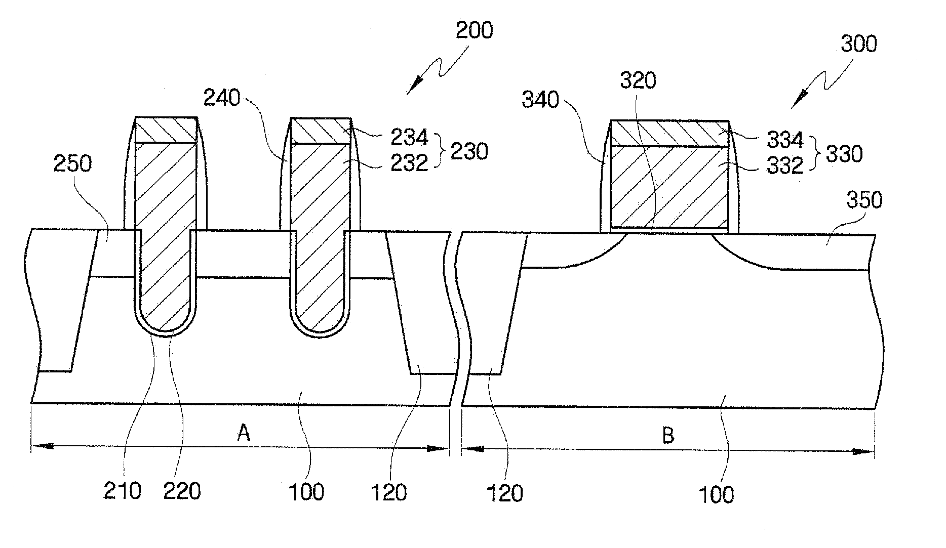
[0024] A method of fabricating the semiconductor integrated circuit device according to an exemplary embodiment of the present invention will now be described in detail with reference to FIG. 1. FIG. 1 is a cross-sectional view of a semiconductor integrated circuit device according to an exemplary embodiment of the present invention.
[0025] Referring to FIG. ...
PUM
 Abstract
Description
Claims
Application Information