Liquid crystal display element

a technology of liquid crystal display and display element, which is applied in non-linear optics, instruments, optics, etc., to achieve the effect of reducing the number of photomasks and the number of irradiation steps

Inactive Publication Date: 2007-02-08
JAPAN SCI & TECH CORP
View PDF1 Cites 13 Cited by
  • Summary
  • Abstract
  • Description
  • Claims
  • Application Information

AI Technical Summary

Benefits of technology

[0037] In the above proof-of-principle experiment, an AFM nano-rubbing was employed for the regulation of the liquid crystal orientation. Alternatively, the same effect can be achieved by an orientation patterning by a photo-alignment using photomasks.
[0038] As described above, in a pattern of a photo mask for dividing into regions, the mask being used for forming multi domains, the pattern itself is optimized so that the symmetry of the head and tail is broken along the orientation axis in each region. Thus, the division into regions and the regulation of pretilt in each region can be achieved at the same time. As a result, the number of irradiation steps and the number of photomasks can be decreased.

Problems solved by technology

The low white luminance is one of the important technical problems in a liquid crystal display device used for a liquid crystal display television which is significantly different from a display device for a computer in which the luminance necessarily has an upper limit in view of asthenopia caused by continuously watching the display for a long time.

Method used


Image

  • Liquid crystal display element
  • Liquid crystal display element
  • Liquid crystal display element

Examples


embodiment 1

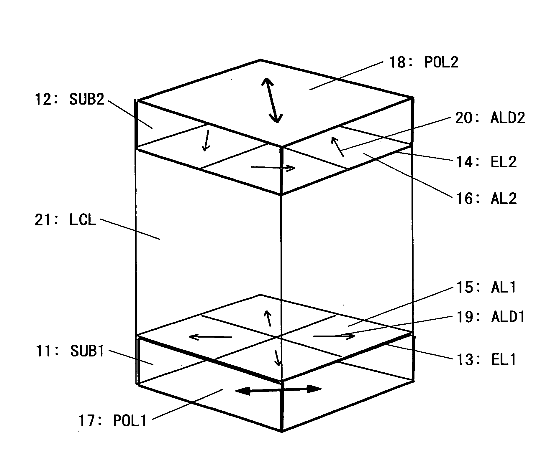
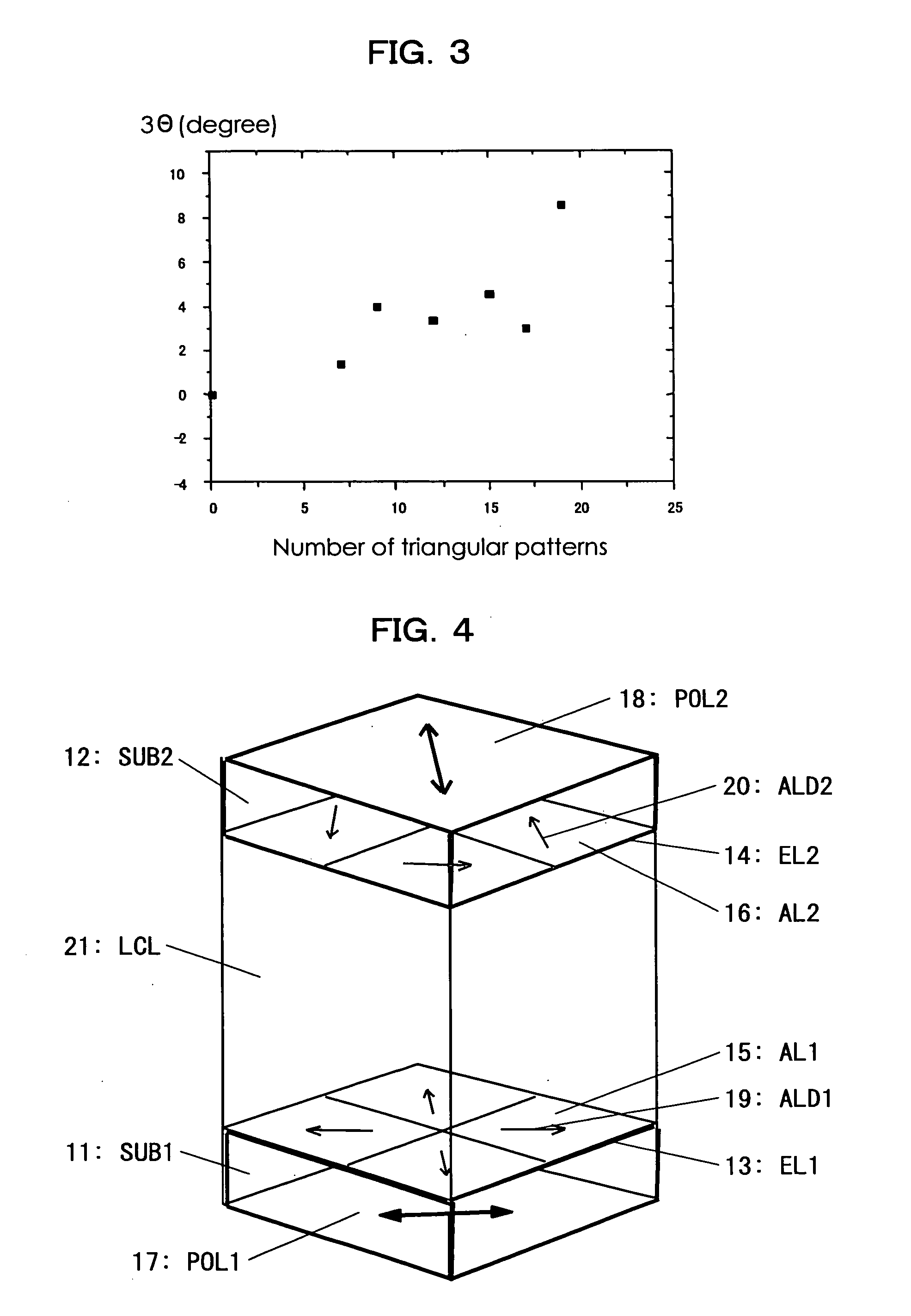
[0051]FIG. 4 is a view showing the structure of a liquid crystal display device according to Embodiment 1 of the present invention.

[0052] In the figure, reference numeral 11 indicates a substrate (SUB1), reference numeral 12 indicates another substrate (SUB2), reference numeral 13 indicates a transparent electrode (EL1), reference numeral 14 indicates another transparent electrode (EL2), reference numeral 15 indicates an alignment layer (AL1), reference numeral 16 indicates another alignment layer (AL2), reference numeral 17 indicates a polarizer (POL1), reference numeral 18 indicates another polarizer (POL2), reference numeral 19 indicates a liquid crystal alignment direction (ALD1), reference numeral 20 indicates another liquid crystal alignment direction (ALD2), and reference numeral 21 indicates a liquid crystal layer (LCL).

[0053] Two transparent glass substrates each having a thickness of 1.1 mm and a polished surface were used as the substrate 11 (SUB1) and the substrate 12 ...

embodiment 2

[0069] Embodiment 2 of the present invention will now be described.

[0070] A liquid crystal display device of Embodiment 2 was fabricated as in Embodiment 1 except for the following. One of the substrates included an alignment layer having the orientation pattern (in FIG. 5) thereon. The other substrate did not include the alignment layer. Furthermore, a chiral dopant CB-15 from Merck & Co., Inc. was added to the liquid crystal material such that the length of helical pitch of the composition corresponded to about ¼ of the cell gap.

[0071] This liquid crystal display device provided the same advantages as those in Embodiment 1 except for the following. In this case, because of the function of the chiral dopant, a TN display structure as in Embodiment 1 was provided in which the liquid crystal orientation was twisted by about 90 degrees between the upper and lower substrates when no voltage was applied.

[0072] According to the measurement of the viewing angle by the same method as in...

embodiment 3

[0073] Embodiment 3 of the present invention will now be described.

[0074] A liquid crystal display device of Embodiment 3 was fabricated as in Embodiment 1 except for the following. In Embodiment 1, the light irradiation was performed two times per substrate using two photomasks shown in FIGS. 5(a) and 5(b) for one substrate, and two photomasks shown in FIGS. 6(a) and 6(b) for the other substrate. Instead, in Embodiment 3, the light irradiation was performed three times per substrate using three photomasks 71 to 73 shown in FIGS. 9(a), 9(b), and 9(c), and three photomasks 81 to 83 shown in FIGS. 9(d), 9(e), and 9(f), respectively.

[0075] Each substrate was irradiated with linearly polarized ultraviolet light with the photomasks shown in FIGS. 9(a), 9(b), and 9(c), or with those shown in FIGS. 9(d), 9(e), and 9(f), in that order. The linearly polarized ultraviolet light was irradiated in the directions diagonal to lines A-A′, B-B′, and A-A′, respectively.

[0076] In Embodiments 1 and...


PUM

PropertyMeasurementUnit
thicknessaaaaaaaaaa
pretilt angleaaaaaaaaaa
thicknessaaaaaaaaaa

Abstract

A liquid crystal display device that can be fabricated more simply as compared with a conventional device and suitably used in a liquid crystal display television satisfying both high pixel transmittance and wide viewing angle display characteristics is provided. The liquid crystal display device includes a pair of substrates including at least one transparent substrate, a liquid crystal layer interposed between the pair of substrates, and a liquid crystal alignment layer interposed between the liquid crystal layer and at least any one of the pair of substrates. On the liquid crystal alignment layer, a plurality of closed regions having a liquid crystal alignment direction different from the surrounding liquid crystal alignment direction are arranged. In the liquid crystal display element, each of the closed regions has such a shape that the head and tail are distinguishable along the surrounding liquid crystal alignment direction.

Description

TECHNICAL FIELD [0001] The present invention relates to a liquid crystal display device, and in particular, to a liquid crystal display device satisfying high transmittance and wide viewing angle range. BACKGROUND ART [0002] Liquid crystal display devices are used as displays for notebook computers, desktop computers, and the like, utilizing their features such as space-saving due to a small thickness, and low power consumption. Furthermore, because of the recent improvement of the technique of producing a liquid crystal panel having a large screen, liquid crystal display devices have also been used as displays for televisions, most of which were hitherto cathode-ray tube-based. Although a twisted nematic (TN) display mode has been mainly used in a liquid crystal display device, the TN display mode cannot provide satisfactory viewing angle characteristics. Accordingly, as such an increase in the screen size of liquid crystal display devices advances, liquid crystal display devices u...

Claims


Application Information

Patent Timeline
Patent Type & Authority Applications(United States)
IPC IPC(8): G02F1/1337G02F1/1333
CPCG02F1/133753G02F2201/14G02F2001/133757G02F1/133788G02F1/133757G02F1/1337
Inventor KIM, JONG-HYUNYONEYA, MAKOTOYOKOYAMA, HIROSHI
Owner JAPAN SCI & TECH CORP
Why Eureka
Try Eureka