Method and system for reshaping metal wires in VLSI design

a metal wire and design technology, applied in the field of very large scale integration (vlsi) circuits, can solve the problems of inability to handle metal wires obtained by conventional chip-level rc extractors, device speed of operation, line-end shortening, etc., and achieve the effect of reducing the time and effort required for rc extraction, facilitating and accelerating rc extraction

Inactive Publication Date: 2007-02-08
RPX CORP
View PDF2 Cites 17 Cited by
  • Summary
  • Abstract
  • Description
  • Claims
  • Application Information

AI Technical Summary

Benefits of technology

[0014] The present invention represents the metal wires in a simplified form and therefore, reduces the time and effort required for RC extraction. Further, the present invention updates the GD by adding data corresponding to the pair of reshaped wires to the GD. The reshaped wires are electrically equivalent and have orth

Problems solved by technology

Specifically, these distortions include line-width variations dependent on pattern density which affect a device's speed of operation and line-end shortening which can break connections to contacts.
Conventional chip-level RC extractors, however, are not able to handle metal wires obtained after OPC.
The methods do not address the side-wall perturbations of metal wires.
Also, the methods discussed above deal with a single wire at a time and are unable to provide a system level solution, whi

Method used


Image

  • Method and system for reshaping metal wires in VLSI design
  • Method and system for reshaping metal wires in VLSI design
  • Method and system for reshaping metal wires in VLSI design

Examples


Embodiment Construction

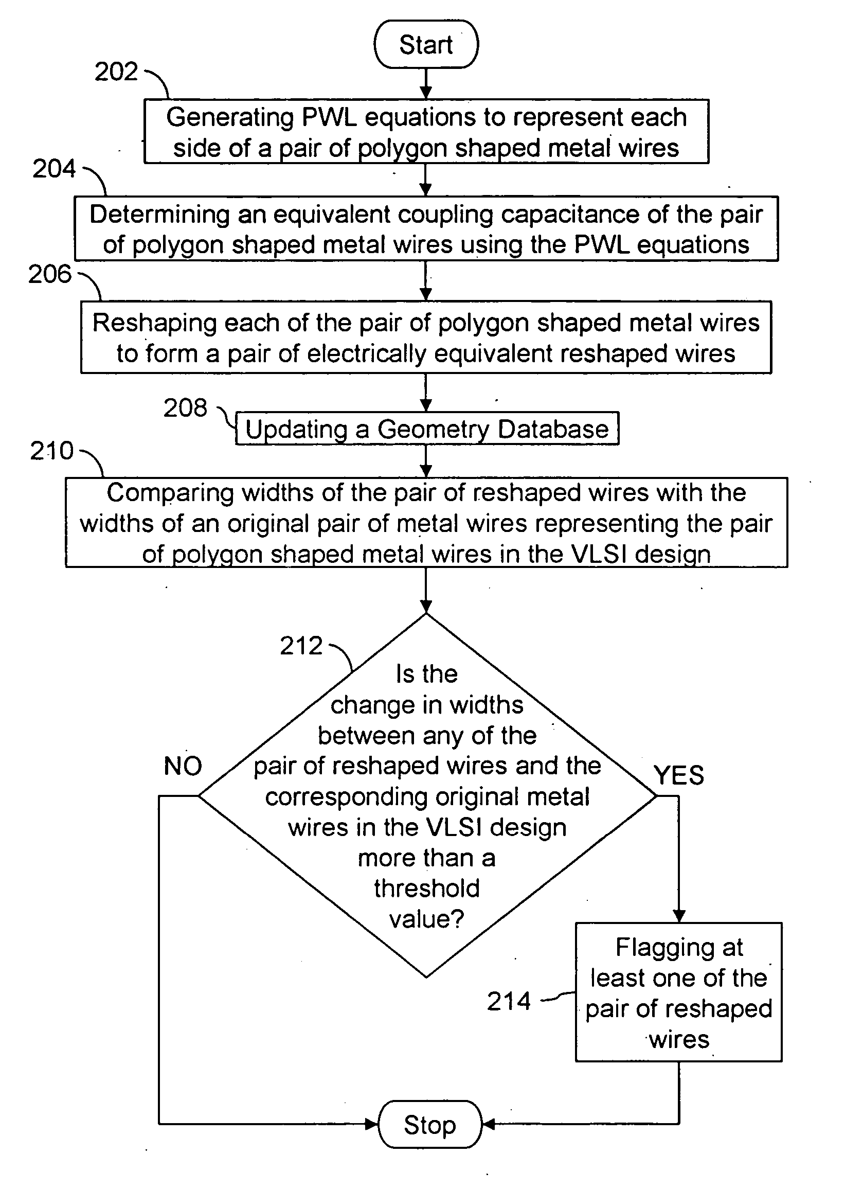
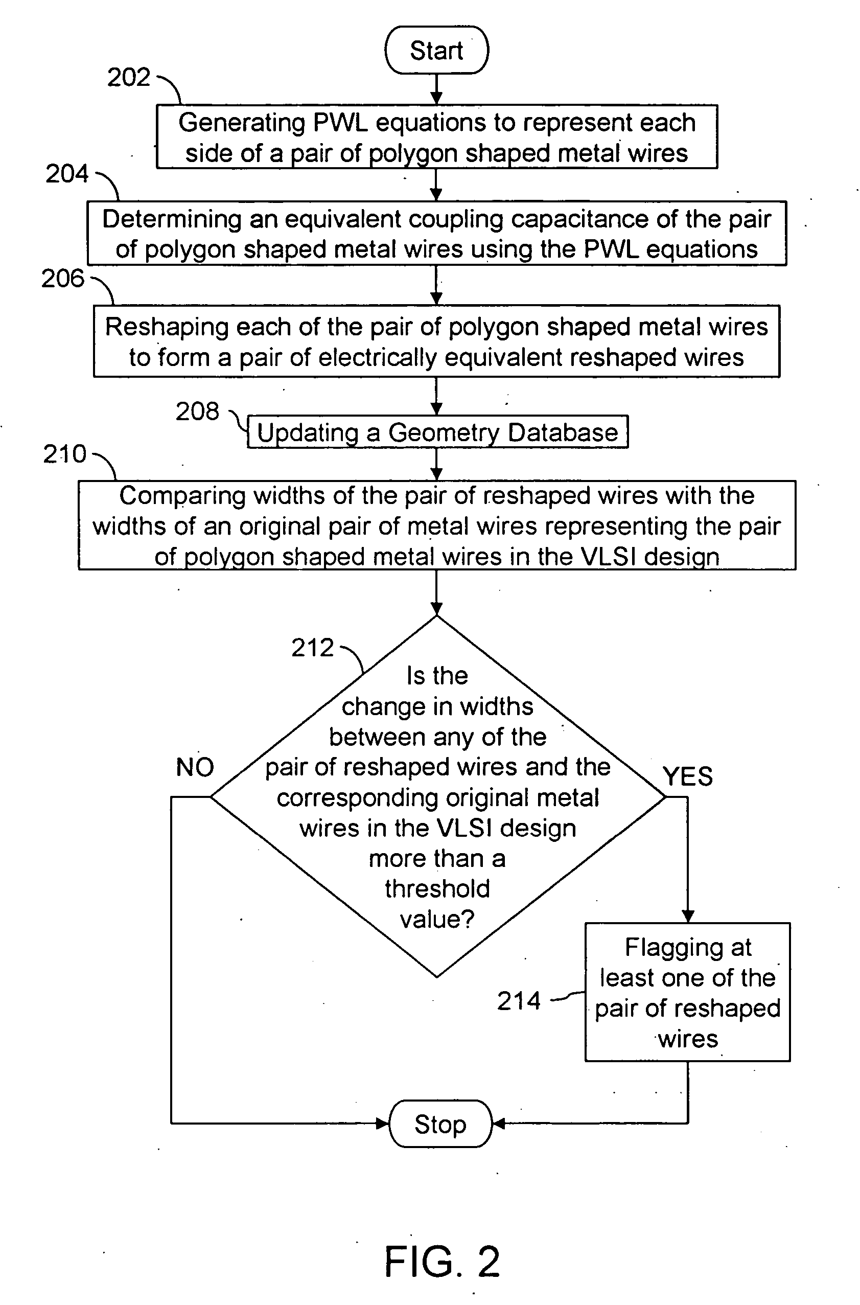
[0028] Various embodiments of the present invention provide a method and a system for reshaping metal wires during Very Large Scale Integration (VLSI) circuit design. A pair of metal wires obtained after Optical Proximity Correction (OPC) is considered at a time. The pair of metal wires is converted into a pair of electrically equivalent reshaped wires. It will be apparent to those skilled in the art that the reshaping is done in design space only. Representations of the metal wires are reshaped in accordance with various embodiments of the present invention. The modified shapes are then stored in a Geometry Database (GD). The modified shapes are then used for Resistance Capacitance (RC) extraction. RC extraction using the modified shapes is quicker and easier as the modified shapes have orthogonal vertices. The shape of the actual metal wires of a VLSI, remain as obtained after OPC.

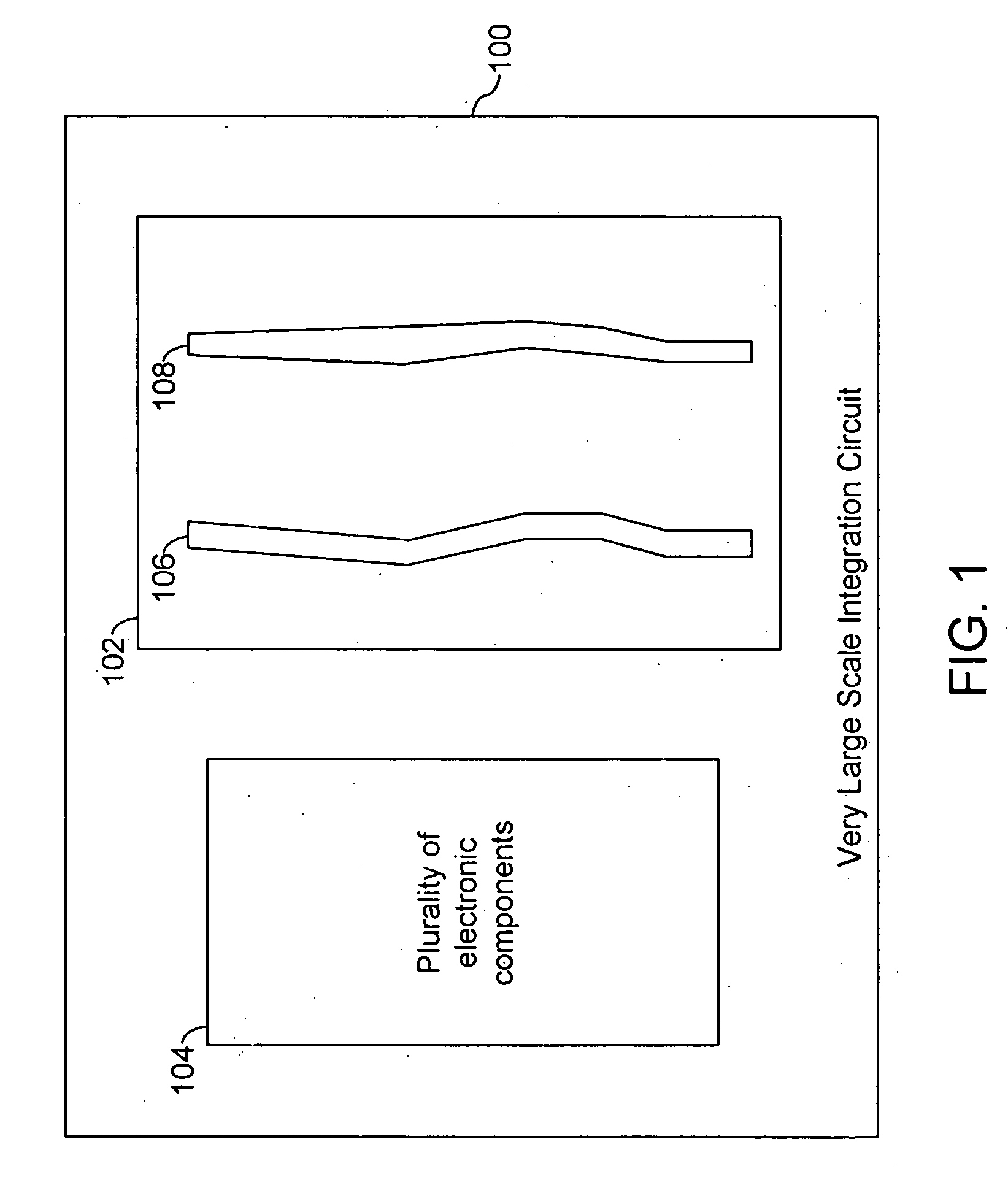
[0029]FIG. 1 illustrates a Very Large Scale Integration (VLSI) circuit 100, in accordance with an em...


PUM


Abstract

A method and system for representing metal wires in Very Large Scale Integration (VLSI) circuit design in a simplified form. A pair of metal wires is considered at a time. A plurality of Piece Wise Linear (PWL) equations is created to represent sides each of the pair of metal wires. The plurality of PWL equations is used to determine an equivalent coupling capacitance of the pair of metal wires. The pair of metal wires is reshaped to form a pair of reshaped metal wires that are electrically equivalent.

Description

BACKGROUND OF THE INVENTION [0001] 1. Field of the Invention [0002] The present invention relates generally to the field of Very Large Scale Integration (VLSI) circuits. More specifically, it relates to the reshaping of metal wires used in VLSI circuits after Optical Proximity Correction to facilitate RC extraction. [0003] 2. Description of the Related Art [0004] Optical Proximity Correction (OPC) is a process for compensating for non-ideal lithography processes. Lithography processes are used to transfer a VLSI circuit design onto a semiconductor wafer. OPC applies systematic changes to photomask geometries to compensate for non-linear distortions caused by optical diffraction and resist process effects. Specifically, these distortions include line-width variations dependent on pattern density which affect a device's speed of operation and line-end shortening which can break connections to contacts. Causes include reticle pattern fidelity, optical proximity effects, and diffusion a...

Claims


Application Information

Patent Timeline
IPC IPC(8): G06F17/50
CPCG06F17/5081G06F30/398
Inventor NAKAGAWA, O. SAMKAHNG, ANDREW B.
Owner RPX CORP
Why Eureka
Try Eureka