Semiconductor Apparatus and Semiconductor Module

a technology of semiconductor modules and semiconductor devices, which is applied in the direction of electrical apparatus, semiconductor devices, semiconductor/solid-state device details, etc., can solve the problems of difficult to dispose circuit elements on top of the back face of the semiconductor substrate, and achieve the effect of improving the mounting efficiency of the devi

Inactive Publication Date: 2007-02-15
SANYO ELECTRIC CO LTD +1
View PDF2 Cites 47 Cited by
  • Summary
  • Abstract
  • Description
  • Claims
  • Application Information

AI Technical Summary

Benefits of technology

[0007] The present invention was conceived in view of such background, and one object of the present invention is to provide a semiconductor apparatus capable of improving the mounting efficiency thereof.

Problems solved by technology

With the semiconductor apparatus being mounted on a circuit board of a subject equipment such as the hand-held equipment there exist substantially no or merely slight gaps between the semiconductor substrate and the circuit board, making it difficult to dispose the circuit element on top of a back face of the semiconductor substrate.

Method used


Image

  • Semiconductor Apparatus and Semiconductor Module
  • Semiconductor Apparatus and Semiconductor Module
  • Semiconductor Apparatus and Semiconductor Module

Examples


Embodiment Construction

[0031] At least the following matters will become apparent from the descriptions of this specification and of the accompanying drawings.

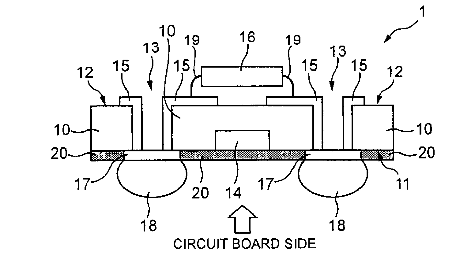
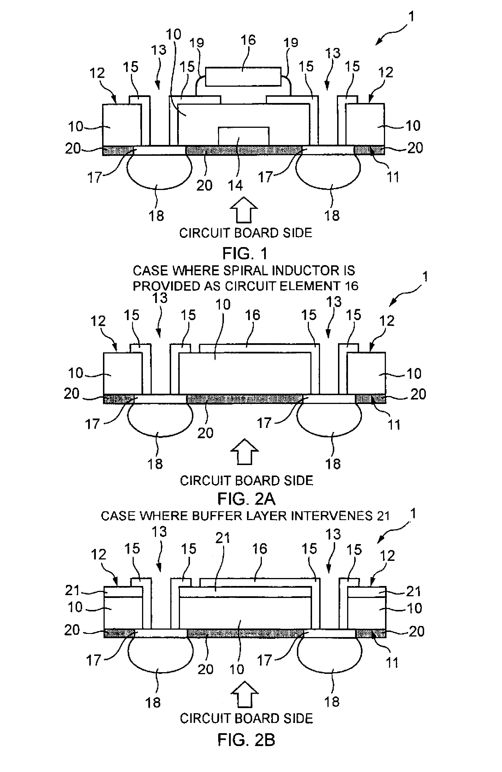
[0032]FIG. 1 shows in diagrammatic section a semiconductor apparatus generally designated at 1 that will now be described as an exemplary embodiment of the present invention. At predetermined locations on a semiconductor substrate 10 made of silicon (Si) are formed through-electrodes 13 extending from a front face 11 to a back face 12 of the semiconductor substrate 10 therethrough. On the front face 11 of the semiconductor substrate 10 is formed an electronic device 14 such as an integrated circuit or a CMOS (Complementary Metal Oxide Semiconductor), linear (bipolar), BiCMOS, MOS or discrete element. The electronic device 14 is formed e.g., by subjecting the semiconductor substrate 10 to various pre-treatments such as thermal oxidation method, CVD (Chemical Vapor Deposition), sputtering, lithography and impurity diffusion.

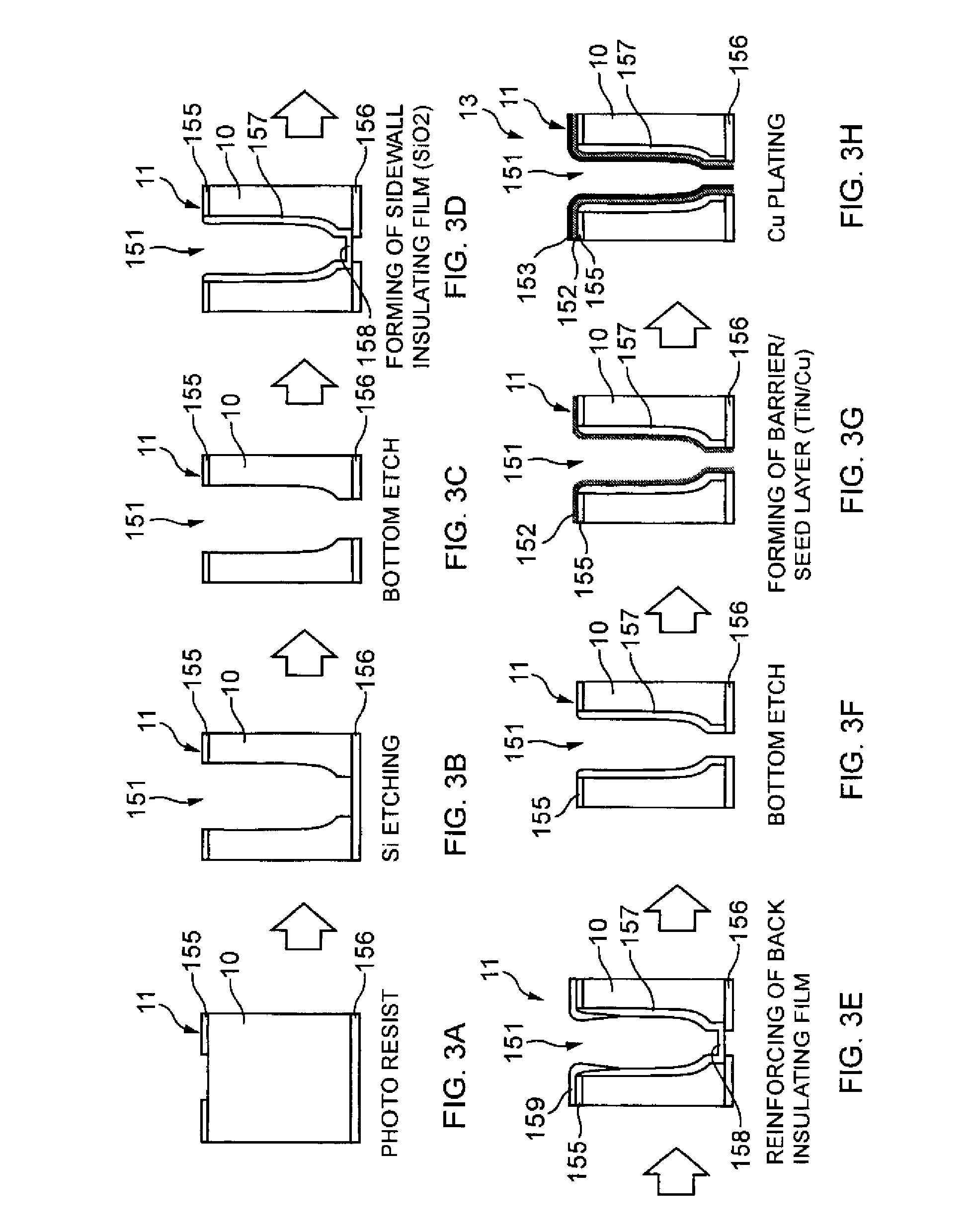
[0033] A wiring pattern (...


PUM


Abstract

A semiconductor apparatus includes a semiconductor substrate, a through-electrode, a solder bump, and a circuit element. The semiconductor substrate has an electronic device formed on its front face. The through-electrode extends through the semiconductor substrate. The solder bump is disposed on the front side of the semiconductor substrate. The circuit element is disposed on the back side of the semiconductor substrate and is connected via the through-electrode to the electronic device.

Description

CROSS-REFERENCE TO RELATED APPLICATIONS [0001] This application claims the benefit of priority from prior Japanese Patent Application Nos. 2004-367523 and 2005-354656, filed Dec. 20, 2004 and Dec. 8, 2005 in Japan, respectively, of which full contents are incorporated herein by reference. BACKGROUND OF THE INVENTION [0002] 1. Field of the Invention [0003] The present invention relates generally to a semiconductor apparatus and a semiconductor module, and more particularly, to a technique for improving the mounting efficiency of the semiconductor apparatus. [0004] 2. Description of the Related Art [0005] With the progress in downsizing and multi-functionalization of the hand-held equipments, the semiconductor apparatuses are facing a need to further improve their mounting efficiencies. For example, Japanese Patent Application Laid-open Publication No. H08-97375 discloses an integrated circuit (IC) such as GaAs MMIC capable of obtaining a desired capacitance value or a desired inducta...

Claims


Application Information

Patent Timeline
Patent Type & Authority Applications(United States)
IPC IPC(8): H01L23/48
CPCH01L21/76898H01L23/481H01L23/5227H01L23/552H01L23/645H01L2924/3025H01L2924/01078H01L2924/01079H01L2924/19103H01L2924/19104H01L2224/16H01L2224/05024H01L2224/05008H01L2224/05009H01L2224/05548H01L2224/05571H01L2224/05001H01L2224/05647H01L2924/00014H01L24/13H01L24/02H01L2224/02372H01L2224/02379H01L2224/13025H01L2224/0557H01L24/05H01L2224/05099
Inventor UMEMOTO, MITSUO
Owner SANYO ELECTRIC CO LTD
Why Eureka
Try Eureka