

Tin-silver solder bumping in electronics manufacture
a technology of tin-silver alloy and electronics, which is applied in the direction of electrolysis components, semiconductor/solid-state device details, electrolysis processes, etc., can solve the problems of low throughput of microelectronic device manufacturers using sn—ag alloy solder wafer bumps, difficult control of ag metal content and uniformity in sn—ag solder wafer bumps, etc., to achieve high current, reduce or eliminate voiding, and ag+
- Summary
- Abstract
- Description
- Claims
- Application Information
AI Technical Summary
Benefits of technology
Problems solved by technology
Method used
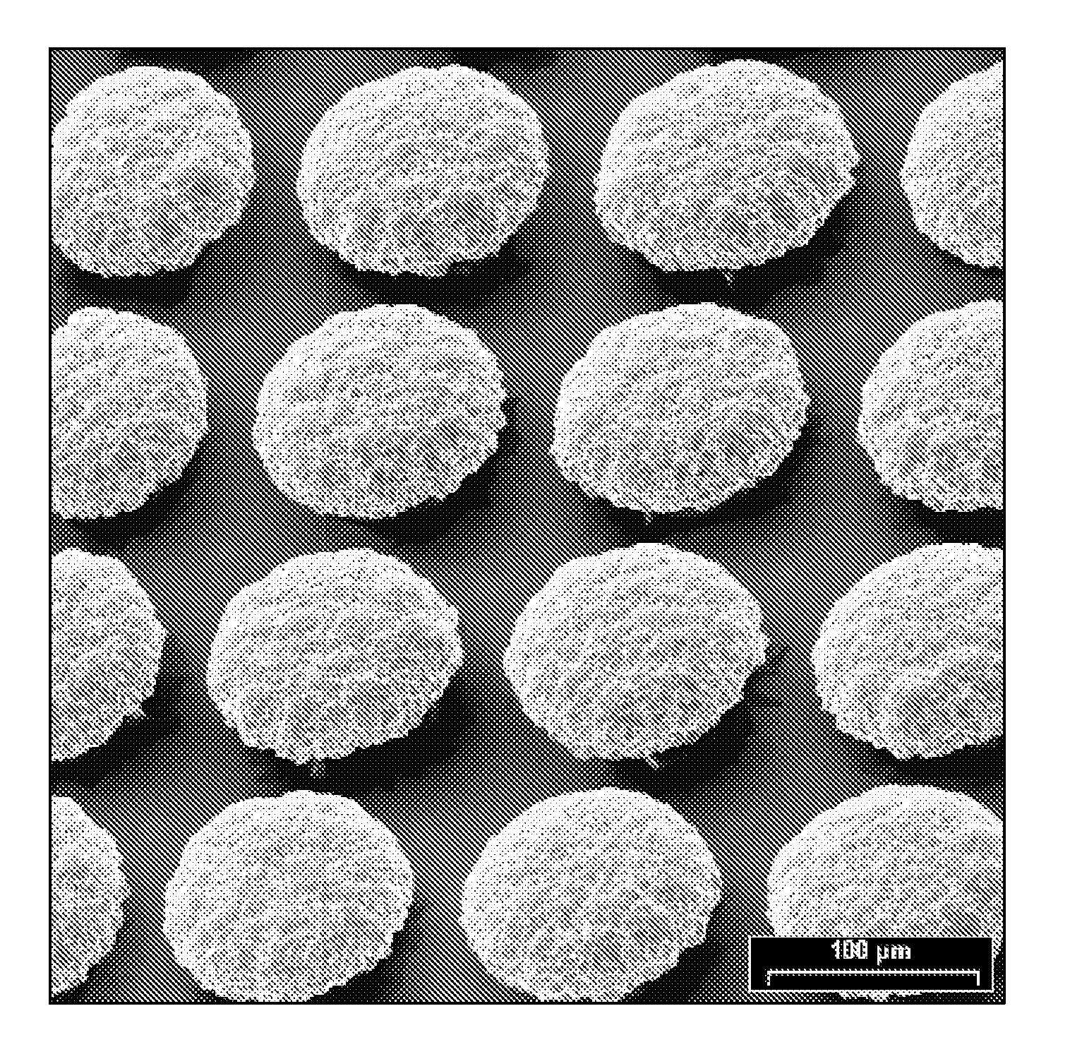
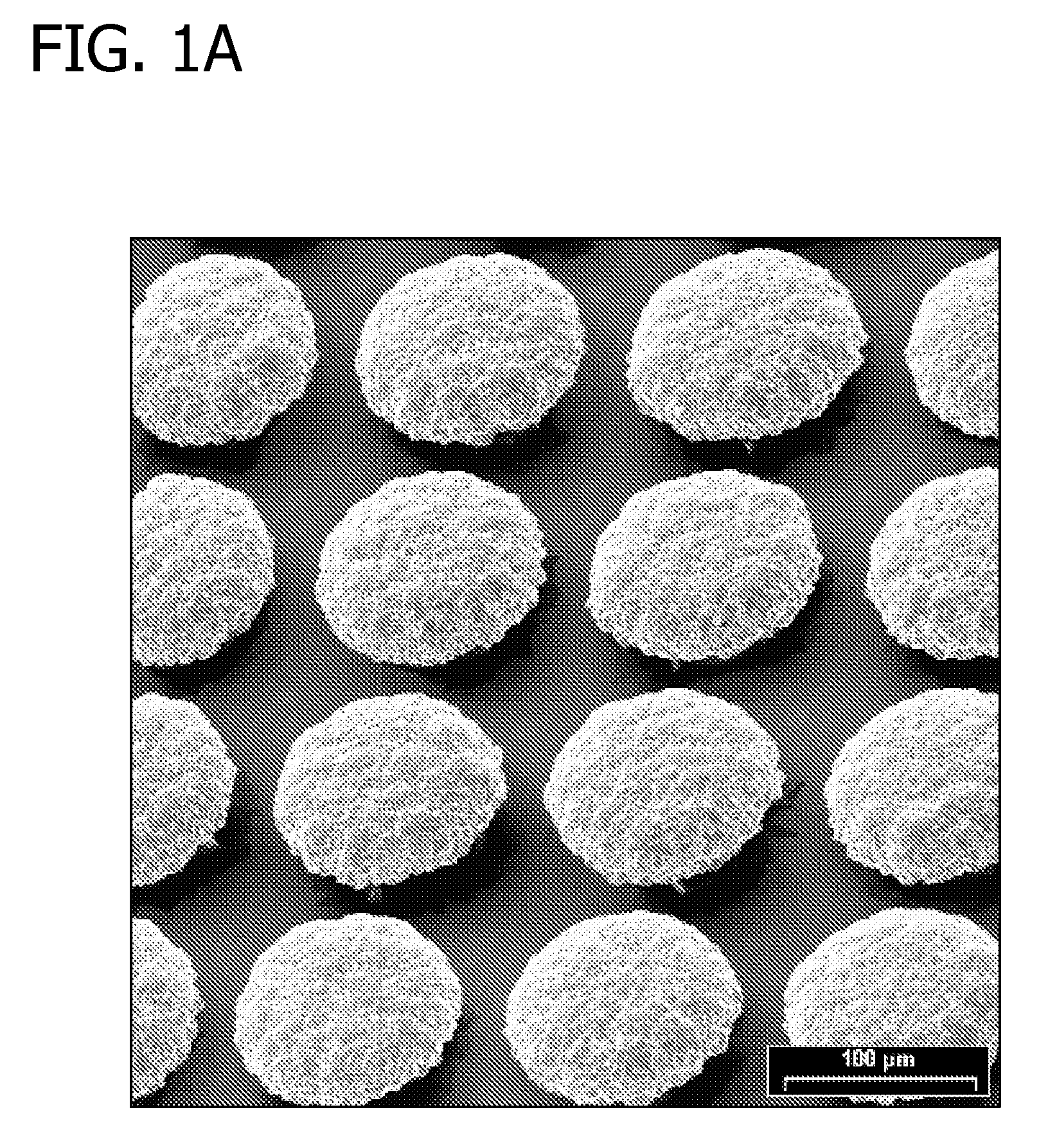
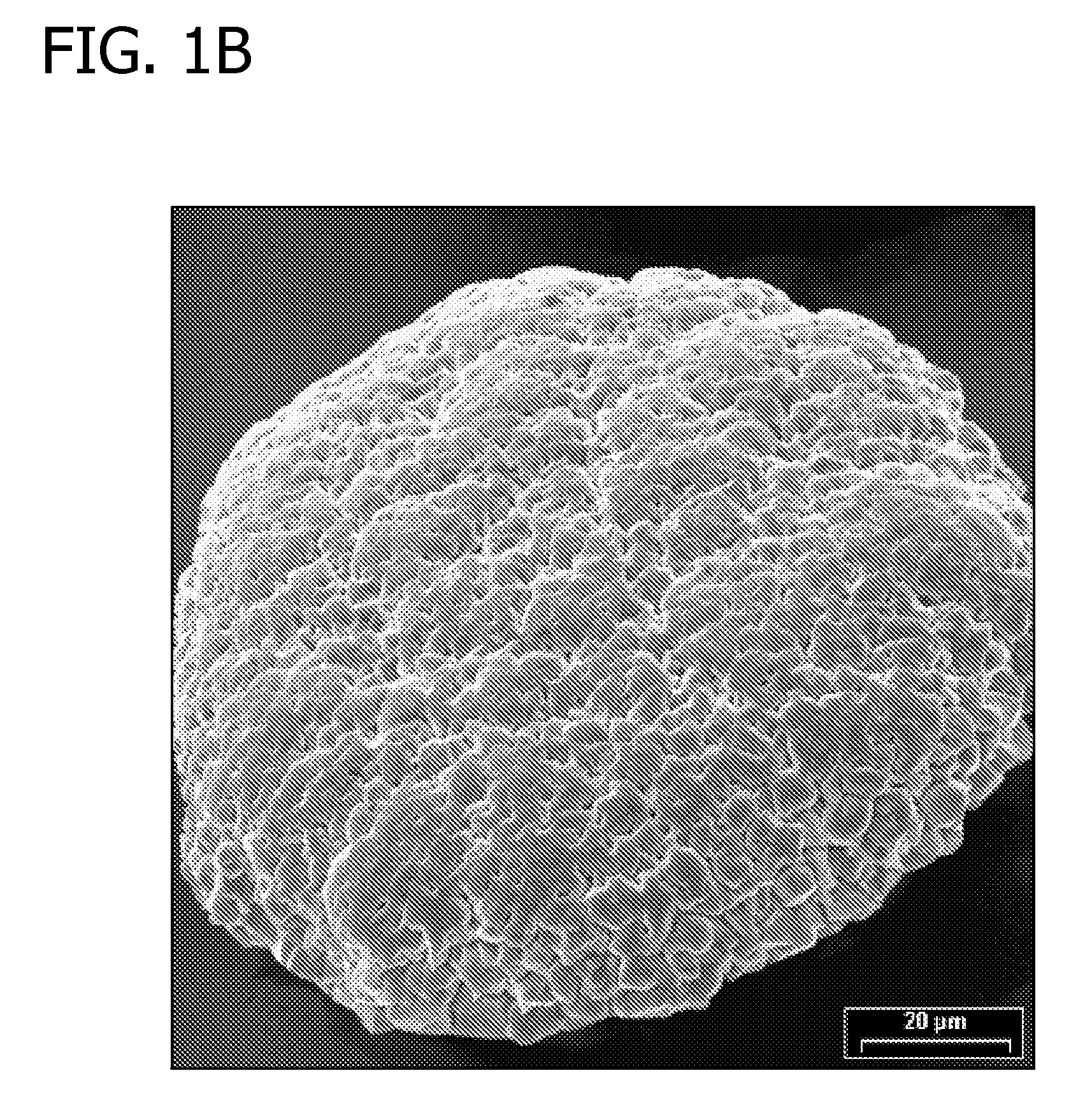
Image

Examples
example 1
Sn—Ag Solder Wafer Bump Electroplating Bath and Method of Preparation
[0052] A Sn—Ag bath for electroplating Sn—Ag alloy solder wafer bumps was prepared comprising the following components: [0053] 2.22 g / L HEAT [0054] 60 g / L Sn2+ as 156 g / L Sn(MSA)2 [0055] 0.5 g / L Ag+ as 0.94 g / L Ag(MSA) [0056] 100 mL / L MSA (70% solution) [0057] 2 g / L Hydroquinone [0058] 7.0 g / L of Lugalvan BNO12 [0059] 1.6 g / L of Dodigen 226 [0060] pH 0
[0061] Optionally, the bath may comprise 0.5 grams per liter of Defoamer SF.
[0062] One liter of this bath was prepared according to the following protocol: [0063] 1) Water (about 400 mL) added to a 1 L flask. [0064] 2) MSA (100 mL of 70% solution) added and solution stirred. [0065] 3) HEAT (2.22 g) added and solution stirred for about 5 minutes. [0066] 4) Ag(MSA) (0.84 g) added and solution stirred for about 5 minutes. [0067] 5) Hydroquinone (2 g) added and solution stirred for about 5 minutes. [0068] 6) Sn(MSA)2 (156 g) added and solution stirred for about 5 minut...
example 2
Sn—Ag Solder Wafer Bump Electroplating Bath
[0073] Another Sn—Ag plating bath was prepared comprising the following components: [0074] 1.75 g / L HEAT [0075] 60 g / L Sn2+ as 156 g / L Sn(MSA)2 [0076] 0.5 g / L Ag+ as 0.94 g / L Ag(MSA) [0077] 100 mL / L MSA (70% solution) [0078] 2 g / L Hydroquinone [0079] 7.0 g / L of Lugalvan BNO12 [0080] 1.6 g / L of Dodigen 226.
example 3
Sn—Ag Solder Wafer Bump Electroplating Bath
[0081] Another bath was prepared comprising the following components: [0082] 2.22 g / L HEAT [0083] 60 g / L Sn2+ as 156 g / L Sn(MSA)2 [0084] 0.5 g / L Ag+ as 0.94 g / L Ag(MSA) [0085] 100 mL / L MSA (70% solution) [0086] 2 g / L Hydroquinone [0087] 7.0 g / L of Lugalvan BNO12 [0088] 1.6 g / L of Dodigen 226 [0089] 0.5 g / L of Defoamer SF.
PUM
| Property | Measurement | Unit |
|---|---|---|
| Concentration | aaaaa | aaaaa |
| Concentration | aaaaa | aaaaa |
| Concentration | aaaaa | aaaaa |
Abstract
Description
Claims
Application Information