
Diode circuit having passive element property, impedance modulator including the diode circuit, and DC source including the diode circuit

Active Publication Date: 2007-02-22
SAMSUNG ELECTRONICS CO LTD
View PDF3 Cites 4 Cited by
  • Summary
  • Abstract
  • Description
  • Claims
  • Application Information

AI Technical Summary

Benefits of technology

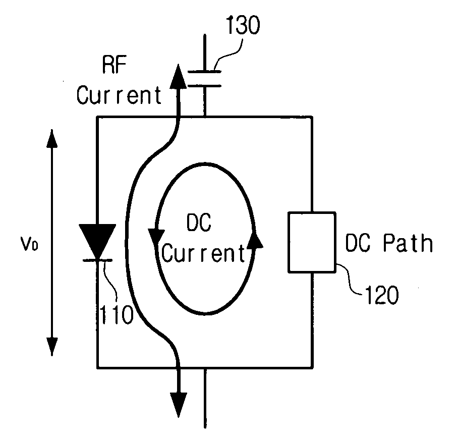
[0008] Accordingly, an aspect of the present invention is to address the above-mentioned problems and make it easier to design an RF circuit by providing a diode circuit, and an impedance modulator and a DC current source that use the diode circuit. More particularly, an aspect of the present invention provides a diode circuit in which the diode is used like a passive element by circulating a DC current generated by a diode along a DC path connected in parallel to the diode.

Problems solved by technology

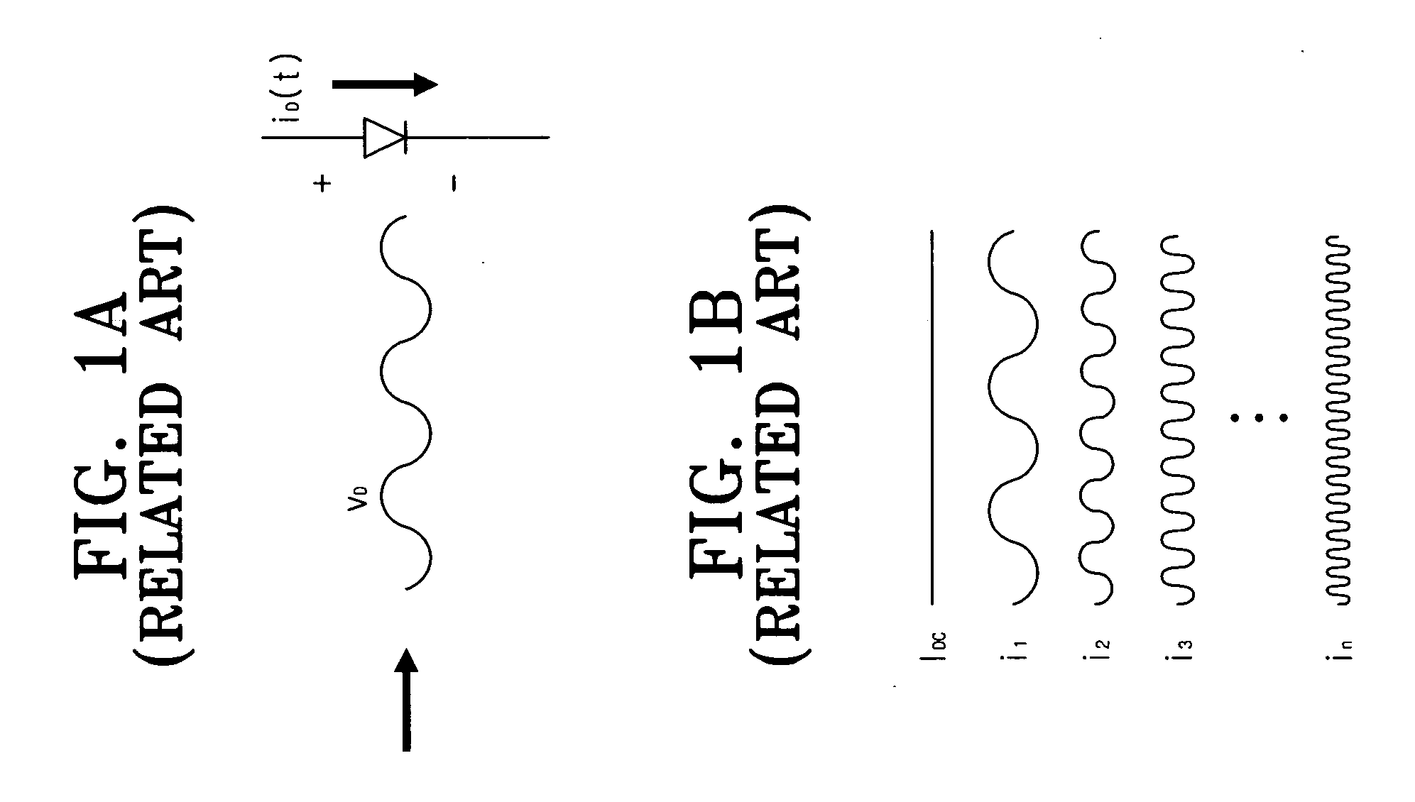
Thus, the diode cannot be used in an RF path where a DC current is intercepted by a capacitor or the like, and this imposes limits on circuit design.

Method used


Image

  • Diode circuit having passive element property, impedance modulator including the diode circuit, and DC source including the diode circuit
  • Diode circuit having passive element property, impedance modulator including the diode circuit, and DC source including the diode circuit
  • Diode circuit having passive element property, impedance modulator including the diode circuit, and DC source including the diode circuit

Examples


Embodiment Construction

[0039] Certain exemplary embodiments of the present invention will be described in greater detail with reference to the accompanying drawings.

[0040] In the drawings, the same elements are denoted by the same reference numerals throughout the drawings. The matters defined in the description such as detailed construction and elements are simply provided to assist in a comprehensive understanding of the invention. Thus, it is apparent that the present invention can be carried out without those defined matters. Also in the following description, detailed descriptions of known functions and configurations incorporated herein have been omitted for conciseness and clarity.

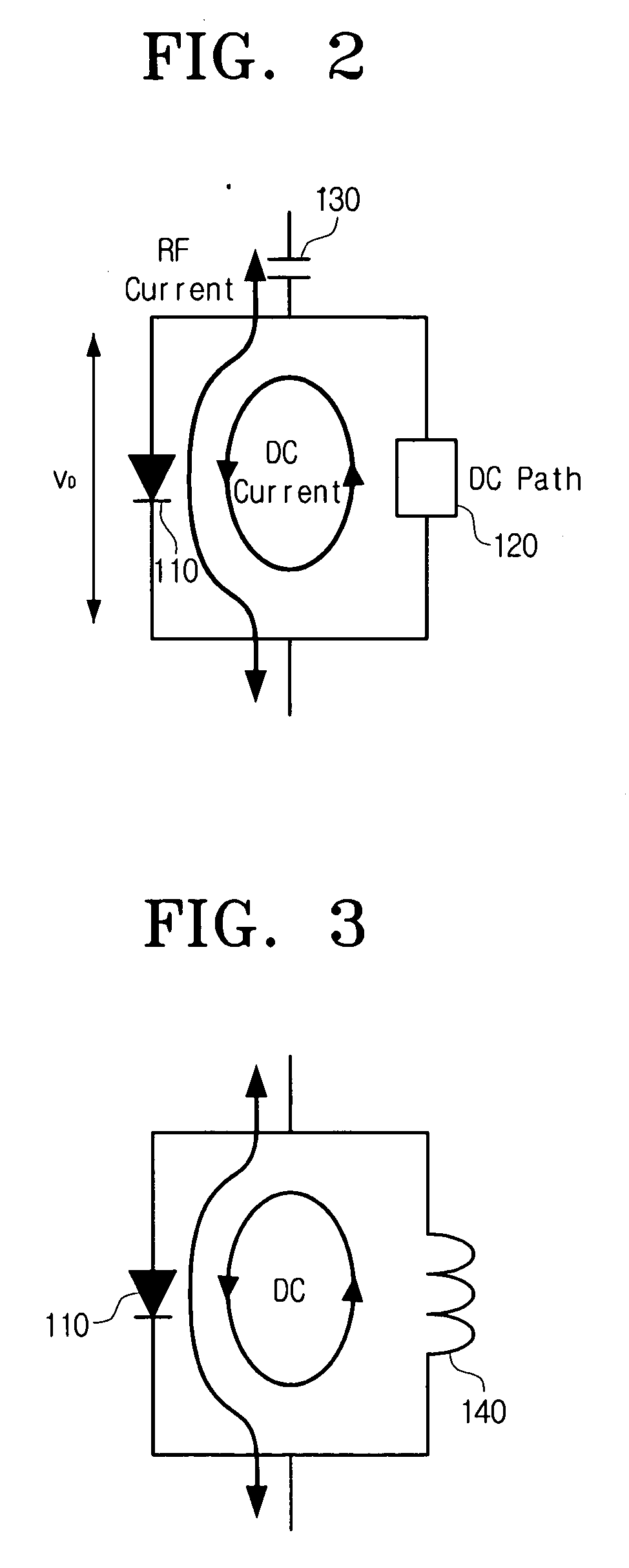
[0041]FIG. 2 is a view that illustrates a configuration of a diode circuit according to an exemplary embodiment of the present invention. Referring to FIG. 2, the diode circuit comprises a first diode 110, a DC path 120, and a DC intercepting capacitor 130.

[0042] The first diode 110 may be a general PN junction diode. ...


PUM


Abstract

A diode circuit having a passive element property, and an impedance modulator and a direct current (DC) source that use the diode circuit are provided. The diode circuit includes a first diode that generates a predetermined DC and alternating currents (AC) when a radio frequency (RF) signal is applied; and a DC path that is connected in parallel to the first diode, forms a predetermined loop and circulates the DC current within the loop. The DC path includes an inductor or an LC parallel resonator. The DC path includes a second diode that is disposed in the opposite direction to the first diode and connected to the first diode in parallel. The present invention can relieve difficulty in designing an RF circuit.

Description

CROSS-REFERENCE TO RELATED APPLICATIONS [0001] This application claims priority from Korean Patent Application No. 10-2005-0046677 filed Jun. 1, 2005, in the Korean Intellectual Property Office, the disclosure of which is incorporated herein by reference. BACKGROUND OF THE INVENTION [0002] 1. Field of the Invention [0003] Apparatus and methods consistent with the present invention relate to a diode circuit having a passive element property, and an impedance modulator and a direct current (DC) source that use the diode circuit, and more particularly, to a diode circuit that has a passive element property by connecting a DC path to a diode and circulating a DC current, and an impedance modulator and a DC source that use the diode circuit. [0004] 2. Description of the Related Art [0005] Various elements of an electronic circuit are classified into active elements or passive elements according to their characteristics. The passive elements consume energy while the active elements supply...

Claims


Application Information

Patent Timeline
IPC IPC(8): H02J3/00
CPCH03F1/56H03F3/19Y10T307/25H01L29/86
Inventor KIM, SEUNG-WOOLEE, SEONG-SOOLEE, JAE-SUP
Owner SAMSUNG ELECTRONICS CO LTD
Learn More