Focus blur measurement and control method

a technology of blur measurement and control method, applied in the field of lithographic process conditions characterization and control, can solve the problems of system error, low-frequency vibration, tilting of across slits, etc., and achieve the effects of improving process parameter monitoring and control, controlling and eliminating blur errors, and improving measurement utilization

Inactive Publication Date: 2007-02-22
GLOBALFOUNDRIES INC
View PDF59 Cites 18 Cited by
  • Summary
  • Abstract
  • Description
  • Claims
  • Application Information

AI Technical Summary

Benefits of technology

[0012] It is another object of the present invention to provide improved utilization of measurements derived from CD metrology tools.
[0013] A further object ...

Problems solved by technology

While defocus and blur can have similar deleterious effects on the quality of the printed image, their cause and means of control are different.
In step and scan lithography, causes of defocus include focus system error, tilts along the scan and slit, wafer non-flatness, lens aberrations such as field curvature and astigmatism, and low-frequency vibration (i.e., where the frequency is less than the scan speed ...

Method used


Image

  • Focus blur measurement and control method
  • Focus blur measurement and control method
  • Focus blur measurement and control method

Examples


Embodiment Construction

)

[0039] In describing the preferred embodiment of the present invention, reference will be made herein to FIGS. 1-14 of the drawings in which like numerals refer to like features of the invention.

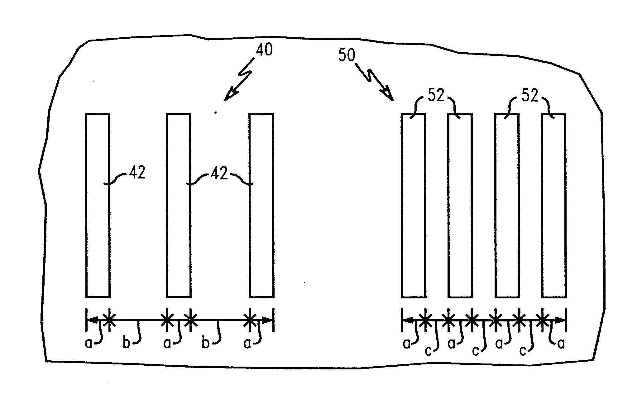
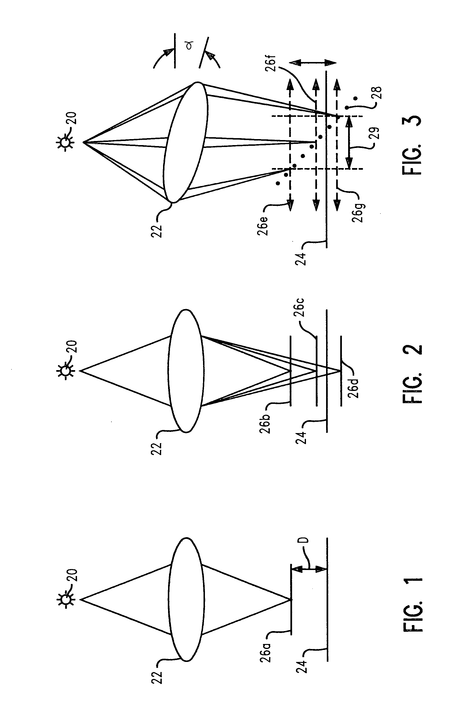
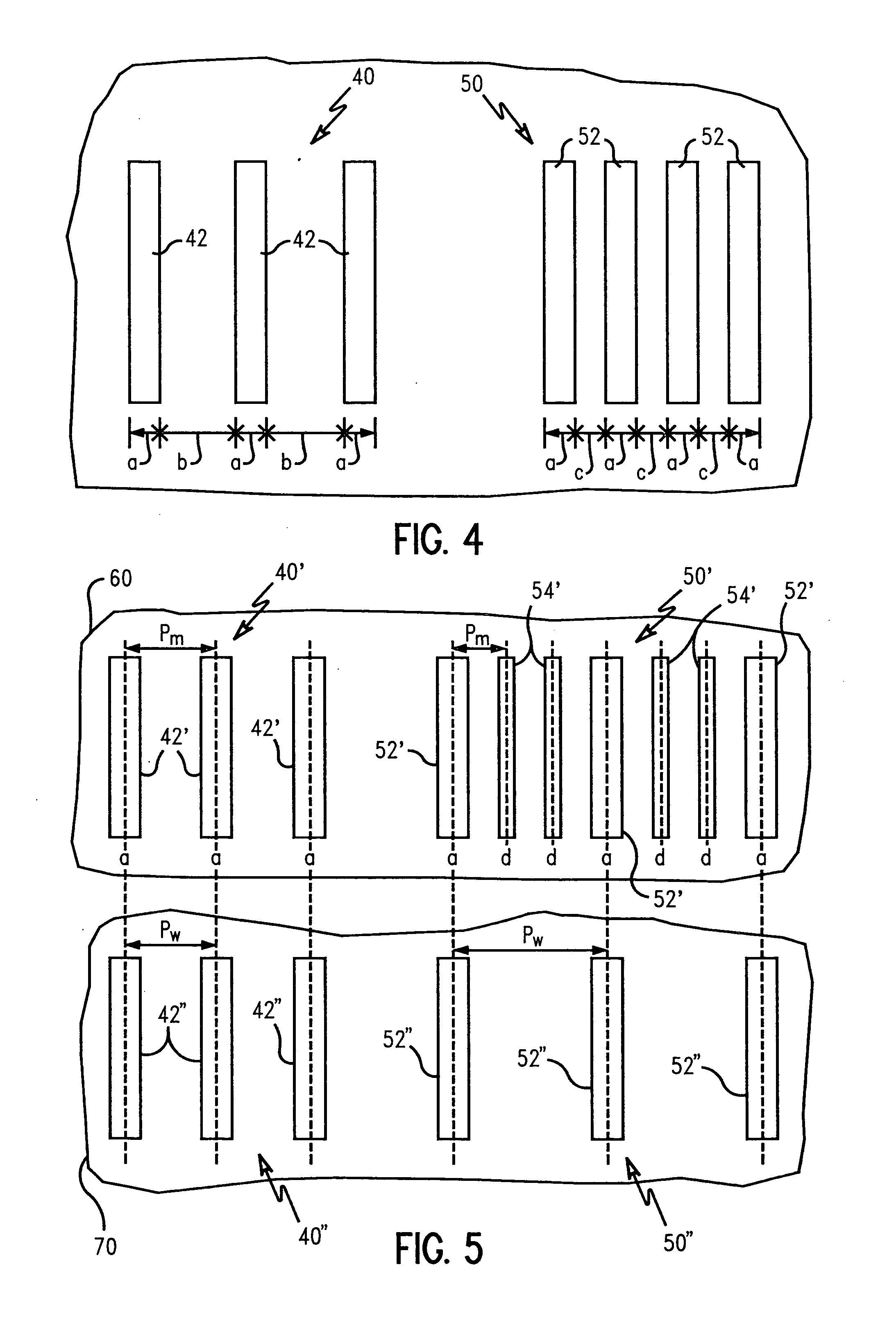
[0040] The inventors of the instant application have found that the response of measurable wafer pattern dimensions to dose, focus and blur errors depends on the mask pattern characteristics defined by various mask dimensions. As used herein, mask pattern dimensions are expressed at the same scale as wafer pattern dimensions. Mask patterns and wafer measurement can be designed to optimize sensitivity to individual dose, focus or blur errors or combinations of thereof. Crucial to the invention is that three or more wafer dimensions, simultaneously or separately measured, have distinguishable responses to the three primary errors: dose, defocus and blur. Ideally, each of the three dimensions would be linearly sensitive to a distinct primary error and insensitive to the other two. In practice...


PUM


Abstract

A method for optimizing imaging and process parameter settings in a lithographic pattern imaging and processing system. The method includes correlating the dimensions of a first set of at least one control pattern printed in a lithographic resist layer, measured at three or more locations on or within the pattern which correspond to differing dose, defocus and blur sensitivity. The method then includes measuring the dimensions on subsequent sets of control patterns, printed in a lithographic resist layer, at three or more locations on or within each pattern, of which a minimum of three locations match those measured in the first set, and determining the effective dose, defocus and blur values associated with forming the subsequent sets of control patterns by comparing the dimensions at the matching locations with the correlated dependencies.

Description

BACKGROUND OF THE INVENTION [0001] 1. Field of the Invention [0002] The present invention relates generally to semiconductor manufacturing and, more particularly, to the characterization and control of lithographic process conditions used in microelectronics manufacturing. [0003] 2. Description of Related Art [0004] During microelectronics manufacturing, a semiconductor wafer is processed through a series of tools that perform lithographic processing, usually followed by etch or implant processing, to form features and devices in the substrate of the wafer. Such processing has a broad range of industrial applications, including the manufacture of semiconductors, flat-panel displays, micromachines, and disk heads. [0005] The lithographic process allows for a mask or reticle pattern to be transferred via spatially modulated light (the aerial image) to a photoresist (hereinafter, also referred to interchangeably as resist) film on a substrate. Those segments of the absorbed aerial imag...

Claims


Application Information

Patent Timeline
IPC IPC(8): G03B27/52
CPCG03F7/70533G03F7/70625G03F7/70641
Inventor AUSSCHNITT, CHRISTOPHER P.BRUNNER, TIMOTHY A.BUTT, SHAHID A.CORLISS, DANIEL A.
Owner GLOBALFOUNDRIES INC
Why Eureka
Try Eureka