Method of manufacturing a thin film transistor matrix substrate

Active Publication Date: 2007-02-22
AU OPTRONICS CORP
View PDF8 Cites 22 Cited by
  • Summary
  • Abstract
  • Description
  • Claims
  • Application Information

AI Technical Summary

Benefits of technology

[0020] (1) The number of required photo masks in the processes is reduced.
[0021] (2) The method is applicable to manufacture inverted staggered back-channel-protected thin film transistor matrix substrates. Due to the inverted staggered back-channel protection, the devices keep their good properties becau

Problems solved by technology

It is well-known that photo masks are expensive.
More photo masks mean a higher cost as well as longer manufacturing time.
However, it is ver

Method used


Image

  • Method of manufacturing a thin film transistor matrix substrate
  • Method of manufacturing a thin film transistor matrix substrate
  • Method of manufacturing a thin film transistor matrix substrate

Examples


Example

[0030] The present invention will be apparent from the following detailed description, which proceeds with reference to the accompanying drawings, wherein the same references relate to the same elements.

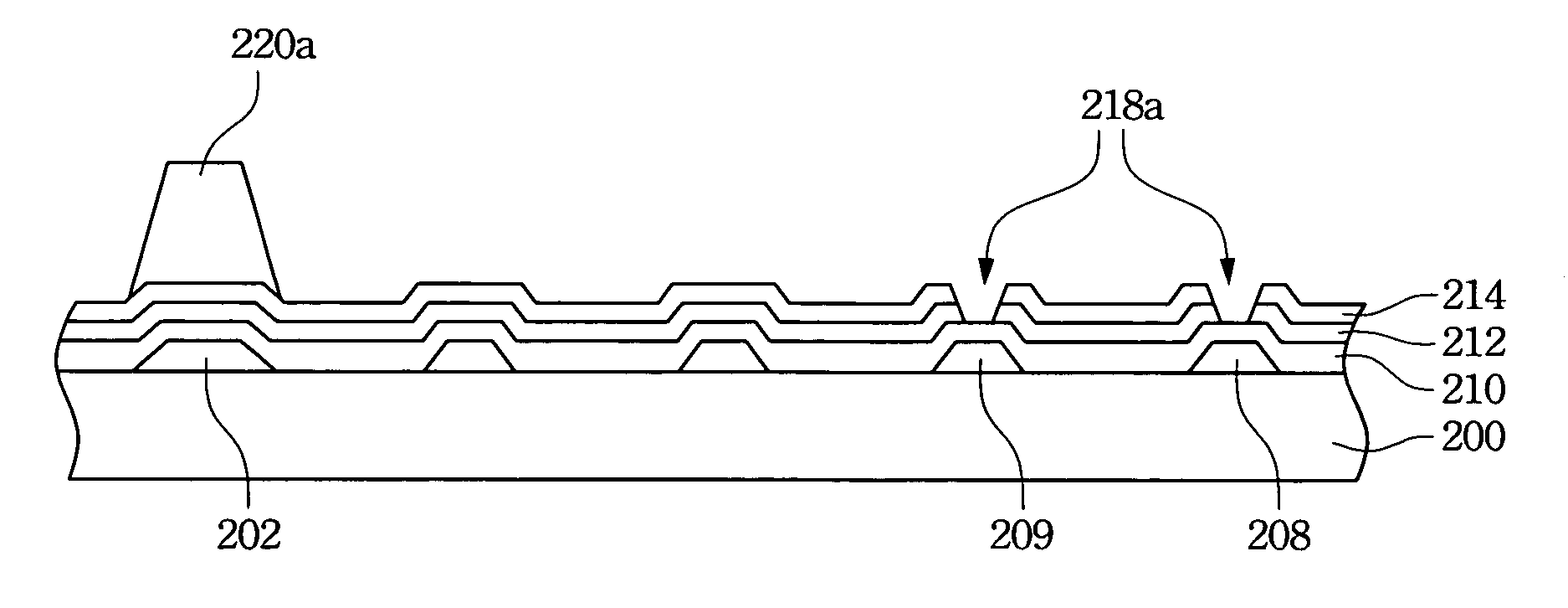
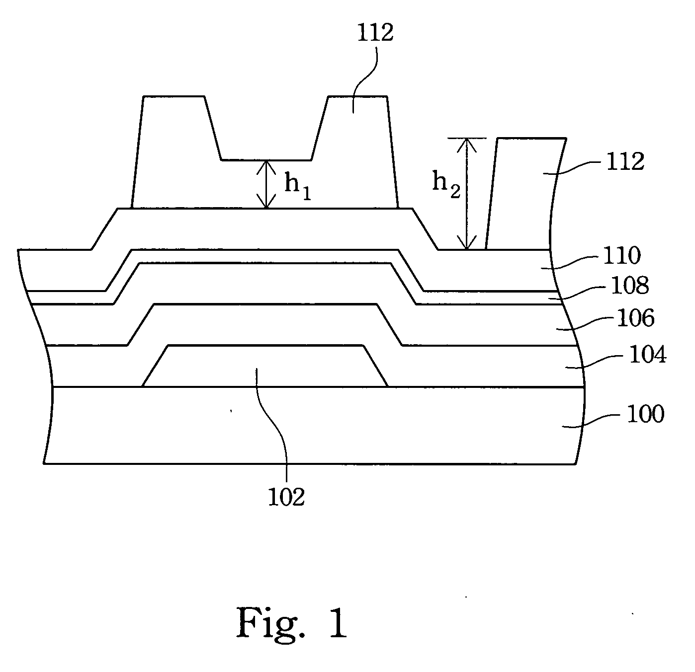
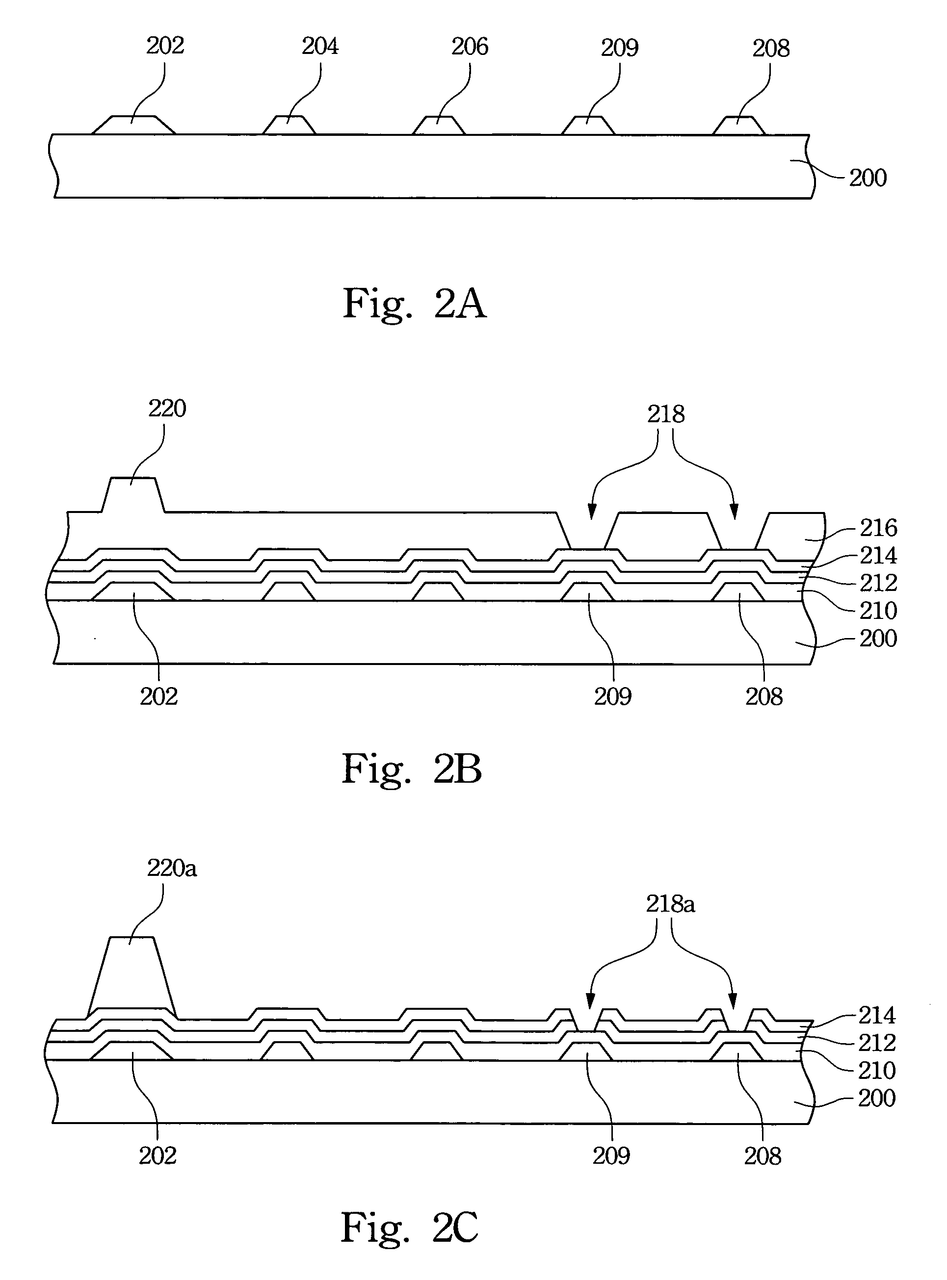
[0031]FIGS. 2A to 2F are schematic cross-sectional views of manufacturing an inverted staggered back-channel-protected thin film transistor matrix substrate according to a preferred embodiment of the invention. As shown in FIG. 2A, a conductive layer is defined on a transparent substrate 200 in a photo mask process, thereby forming a gate electrode 202, a lower electrode of a storage capacitor 204, a signal electrode 206, and a gate electrode pads 208, and signal electrode pads 209. The transparent substrate 200 is a glass substrate. The material of the conductive layer is Al, Mo, Cu, alloys thereof, and metal nitrides. The conductive layer may have a single-layer or a multi-layer structure formed from the above-mentioned materials.

[0032] With reference to FIG. 2B, the transparent ...


PUM


Abstract

A method of manufacturing a thin film transistor matrix substrate is provided. The first photo-mask process is used to define a gate electrode and a signal electrode. The second photo-mask process is used to obtain different thickness of a PR layer in different regions for forming a channel, gate electrode through holes, signal electrode through holes and conductive pads. The third photo-mask process is used to define a source, a drain, an upper signal electrode, a pixel electrode, gate electrode pads and signal electrode pads.

Description

RELATED APPLICATIONS [0001] The present application is based on, and claims priority from, Taiwan Application Serial Number 94128098, filed Aug. 17, 2005, the disclosure of which is hereby incorporated by reference herein in its entirety. BACKGROUND OF THE INVENTION [0002] 1. Field of Invention [0003] The invention relates to a method of manufacturing a liquid crystal display (LCD) panel and, in particular, to a method of manufacturing a thin film transistor matrix substrate. [0004] 2. Related Art [0005] In recent years, opto-electronic related technologies have made tremendous progress. The digital era promotes the development of the LCD market. Since they have such advantages as high picture quality, small size, light weight, low driving voltages, and low power consumption, the LCD's have been widely used in personal digital assistants (PDA), mobile phones, camcorders, notebook computers, desktop displays, vehicle displays, and projection televisions. They have gradually replaced ...

Claims


Application Information

Patent Timeline
IPC IPC(8): H01L21/84H01L21/00
CPCG02F2001/136236H01L27/124H01L27/1288G02F1/136236
Inventor LEE, LIU-CHUNG
Owner AU OPTRONICS CORP
Why Eureka
Try Eureka