Photoelectric conversion device and imaging device

a conversion device and imaging device technology, applied in the direction of photoelectric discharge tubes, instruments, material analysis, etc., can solve the problems of increased leakage current which is considered, increased s/n, and increased s/n, etc., to achieve low resistance, large light transmittance, and low resistance

Inactive Publication Date: 2007-03-01
FUJIFILM CORP +1
View PDF6 Cites 18 Cited by
  • Summary
  • Abstract
  • Description
  • Claims
  • Application Information

AI Technical Summary

Benefits of technology

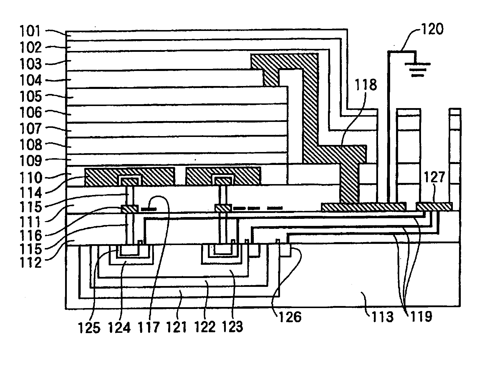
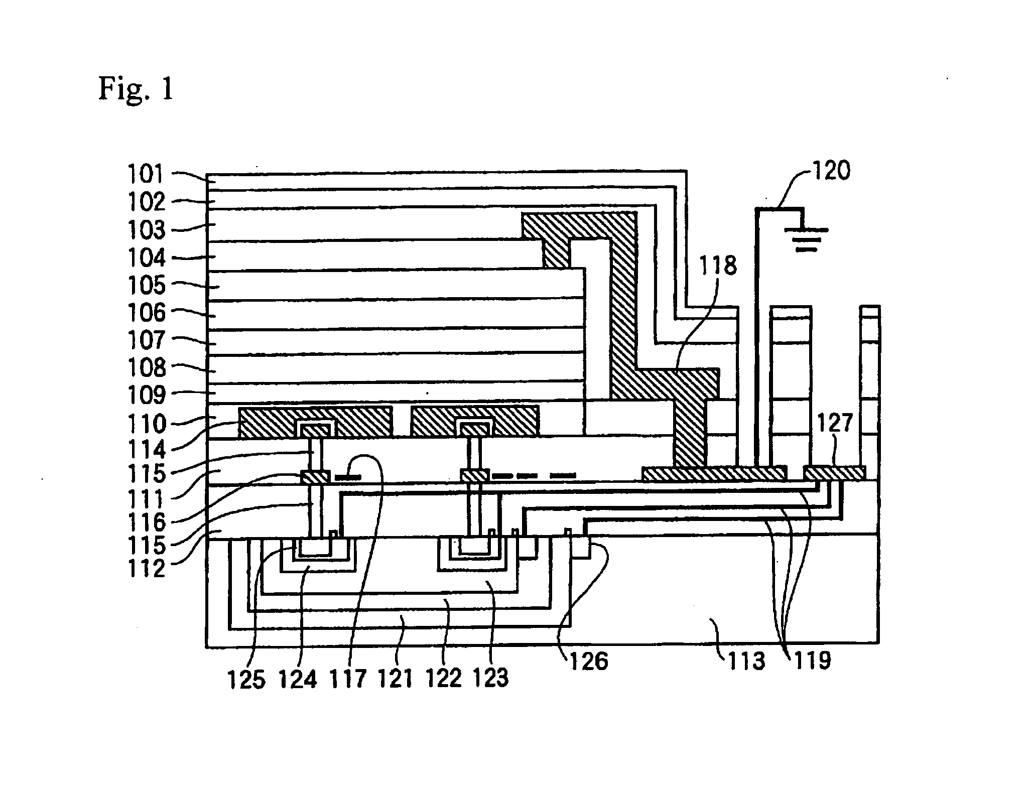
[0018] The effect of the invention is remarkably revealed in the case where a minuter layer is applied as the transparent conducting thin layer. It is thought that a transparent conducting oxide (TCO) is preferable as the transparent conducting thin layer because of its high light transmittance and low resistivity. In general, since in a transparent conducting oxide (TCO) layer, a minute layer is formed against a metal thin layer of Al, etc., the effect of the invention is remarkably revealed.
[0019] The effect of the invention is especially remarkable against a photoelectric conversion layer including a crystalline layer (namely, grain boundary-containing layer) in which cracks are likely formed. In the case where an organic thin layer is applied as the photoelectric conversion layer, when a pigment based material is contained in the photoelectric conversion layer, the effect of the invention is large. Furthermore, since the non-uniformity of the layer increases, when the thickness due to the pigment based material increases, the effect of the invention becomes larger. In order to bring light absorption or sufficient photoelectric conversion performance, it is better that the thickness of the pigment based material is thick within a certain range. The thickness of the pigment based material is preferably 75 nm or more, and more preferably 100 nm or more (preferably not more than 1,000 nm). The grain boundary is confirmed by an electron microscope or the like.
[0020] Examples of the pigment based material include usual pigments, namely organic pigments and inorganic pigments. In the invention, such a material is a substance which is substantially insoluble in water or an organic solvent and which is capable of forming the foregoing crystalline layer. Furthermore, even a substance which is soluble in water or an organic solvent is included so far as it is used in a solid state, thereby forming a crystalline layer. The pigment based material is preferably an organic pigment, and examples of the organic pigment include dyes as described later. That is, pigments among the p-type organic dyes or n-type organic dyes are preferably used.
[0021] In the case where an organic layer is supposed as the photoelectric conversion layer, when the transparent conducting thin layer is subjected to film formation by a usual sputtering method or the like, there is some possibility that the performance of the photoelectric conversion layer is deteriorated by the damage by plasma. For that reason, the film formation of the transparent conducting thin layer is preferably carried out by a plasma-free method. Here, the term “plasma-free state” means a state that plasma is not generated during the film formation of a transparent electrode layer, or a distance from the plasma generation source to the substrate is 2 cm or more, preferably 10 cm or more, and more preferably 20 cm or more and that the plasma which reaches the substrate is reduced.
[0022] Examples of a device in which plasma is not generated during the film formation of a transparent electrode layer include an electron beam vapor deposition device (EB vapor deposition device) and a pulse laser vapor deposition device. With respect to the EB vapor deposition device or pulse laser vapor deposition device, devices as described in Developments of Transparent Conducting Films, supervised by Yutaka Sawada (published by CMC Publishing Co., Ltd., 1999); Developments of Transparent Conducting Films II, supervised by Yutaka Sawada (published by CMC Publishing Co., Ltd., 2002); Technologies of Transparent Conducting Films, written by Japan Society for the Promotion of Science (published by Ohmsha, Ltd., 1999); and references as added therein can be used. In the following, the method for achieving film formation of a transparent electrode film using an EB vapor deposition device is referred to as “EB vapor deposition method”; and the method for achieving film formation of a transparent electrode film using a pulse laser vapor deposition device is referred to as “pulse laser vapor deposition method”.
[0023] With respect to the device capable of realizing the state that a distance from the plasma generation source to the substrate is 2 cm or more and that the plasma which reaches the substrate is reduced (hereinafter referred to as “plasma-free film formation device”), for example, a counter target type sputtering device and an arc plasma vapor deposition method can be thought. With respect to these matters, devices as described in Developments of Transparent Conducting Films, supervised by Yutaka Sawada (published by CMC Publishing Co., Ltd., 1999); Developments of Transparent Conducting Films II, supervised by Yutaka Sawada (published by CMC Publishing Co., Ltd., 2002); Technologies of Transparent Conducting Films, written by Japan Society for the Promotion of Science (published by Ohmsha, Ltd., 1999); and references as added therein can be used.

Problems solved by technology

In that case, in comparison with an Al electrode and so on, an increase of the leakage current which is considered to be caused due to an increase of a short circuit part is liable to be generated.
Also, there are caused problems such as deterioration of S / N, scattering of the performance, and the generation of a complete DC short circuit so that the device does not drive according to circumstances.
In this way, though there may be the case where the increase of the leakage current can be reduced, there was some possibility that the introduction of such a protective layer causes the deterioration of other performances of the device.
However, in that case, the light transmittance of the layer itself is low so that it cannot be said that this electrode is a transparent electrode; the light incidence is achieved by providing an opening; and this patent document does not mention the thickness and ratio of the photoelectric conversion layer and a transparent conducting layer as stacked thereon into which the light can be made incident.

Method used


Image

  • Photoelectric conversion device and imaging device
  • Photoelectric conversion device and imaging device

Examples


example 1

[0094] In the foregoing preferred photoelectric conversion device structure, ITO was used as the transparent pixel electrode 114 of each of the invention and the comparison, and its thickness was 100 nm. ITO was used as the transparent electrode 105 of each of the invention and the comparison, and its thickness was 10 nm for the invention and 50 nm for the comparison, respectively. With respect to the film formation method the transparent pixel electrode, an RF magnetron sputtering method (TS distance: 10 cm) was employed, the amount of introduction of O2 was 0%, and the temperature at the time of film formation was 25° C. On the other hand, with respect to the transparent electrode of the invention, an RF magnetron sputtering method (TS distance: 10 cm) was employed, the amount of introduction of O2 was 0%, the temperature at the time of film formation was 25° C., and the time for the film formation was 4 minutes and 50 seconds (290 seconds). With respect to the transparent electro...


PUM


Abstract

A photoelectric conversion device comprising: a substrate; a conducting layer; a photoelectric conversion layer; and a transparent conducting layer provided in this order, wherein the transparent conducting layer has a thickness of not more than ⅕ of that of the photoelectric conversion layer.

Description

[0001] The present invention relates to a solid imaging device including a transparent electrode in an upper part of a photoelectric conversion layer and provides a solid imaging device which is high in sensitivity and low in noise and which is high in yield. BACKGROUND OF THE INVENTION [0002] In a photoelectric conversion device which is made of a photoelectric conversion part having a transparent electrode formed thereon, for the purpose of increasing the absolute amount of incident light into the photoelectric conversion part to enhance the carrier read-out efficiency after the photoelectric conversion, there have hitherto been demanded ones having a higher light transmittance of the transparent electrode. In the case of taking into consideration such high light transmittance and low resistance value, it is generally thought that a transparent conducting oxide (TCO) thin layer is preferable. In general, the formation of a TCO transparent electrode is carried out by a sputtering m...

Claims


Application Information

Patent Timeline
Patent Type & Authority Applications(United States)
IPC IPC(8): H01L31/00H03F3/08
CPCH01L27/1462H01L31/022466H01L27/14645H01L27/14632H01L31/022475
Inventor MITSUI, TETSURO
Owner FUJIFILM CORP
Why Eureka
Try Eureka