Semiconductor device and manufacturing method thereof

a technology of semiconductors and semiconductors, applied in the direction of thermoelectric devices, electroluminescent light sources, electric lighting sources, etc., can solve the problems of difficult manufacturing and inability to form tfts using plastic films, and achieve the effects of low adhesion, high adhesion and high yield

Active Publication Date: 2007-03-01
SEMICON ENERGY LAB CO LTD
View PDF8 Cites 72 Cited by
  • Summary
  • Abstract
  • Description
  • Claims
  • Application Information

AI Technical Summary

Benefits of technology

[0032] In the present invention, since the adhesion between the inorganic compound layer and the conductive layer is higher than that between the layer containing an organic compound and the conductive layer, separation is difficult to occur at an interface between the inorganic compound layer and the conductive layer in a separation step. Therefore, by forming a region having low adhesion and a region having high adhesion so as to surround an outer edge of the region having low adhesion when viewed from above, separation at an interface between the conductive layer and the layer containing an organic compound can be prevented. Moreover, a layer having a storage element or a light-emitting element formed over a substrate can be separated with high yield. Further, a semiconductor device provided with an element which has a layer containing an organic compound over a flexible substrate can be manufactured with high yield.
[0033] In a semiconductor device of the present invention, a layer containing an organic compound and an organic insulating layer are sandwiched between an inorganic compound layer and a conductive layer, and moreover, the semiconductor device has a number of regions where the inorganic compound layer and the conductive layer are in contact with each other. Thus, regions where the layer containing an organic compound and the organic insulating layer are exposed to the air decrease and moisture, oxygen, and the like are unlikely to intrude such regions. This makes it possible to suppress deterioration of the semiconductor device.
[0034] Since a semiconductor device provided with an element which has a layer containing an organic compound over a flexible substrate can be obtained, the semiconductor device can be more lightweight and thinner.

Problems solved by technology

Therefore, TFTs cannot be formed using a plastic film to have as favorable electrical characteristics as those formed over a glass substrate.
As a result, it is difficult to manufacture, with high yield, semiconductor devices in each of which the element which has the layer containing an organic compound is provided over a plastic substrate.

Method used


Image

  • Semiconductor device and manufacturing method thereof
  • Semiconductor device and manufacturing method thereof
  • Semiconductor device and manufacturing method thereof

Examples


embodiment modes

[0058] Embodiment modes and embodiments of the present invention will hereinafter be described with reference to drawings. However, the present invention is not restricted to the following description, and it is easily understood by those skilled in the art that the mode and detail can be variously changed without departing from the scope and spirit of the present invention. Therefore, the present invention is not restricted to the description of the embodiment modes and embodiments hereinafter shown. It is to be noted that, in the structure of the present invention hereinafter described, the reference numeral indicating the same part is used in common throughout the drawings.

embodiment mode 1

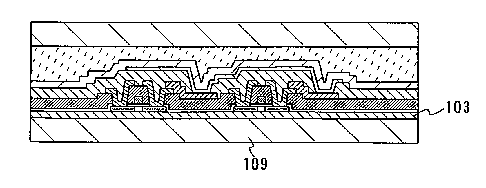
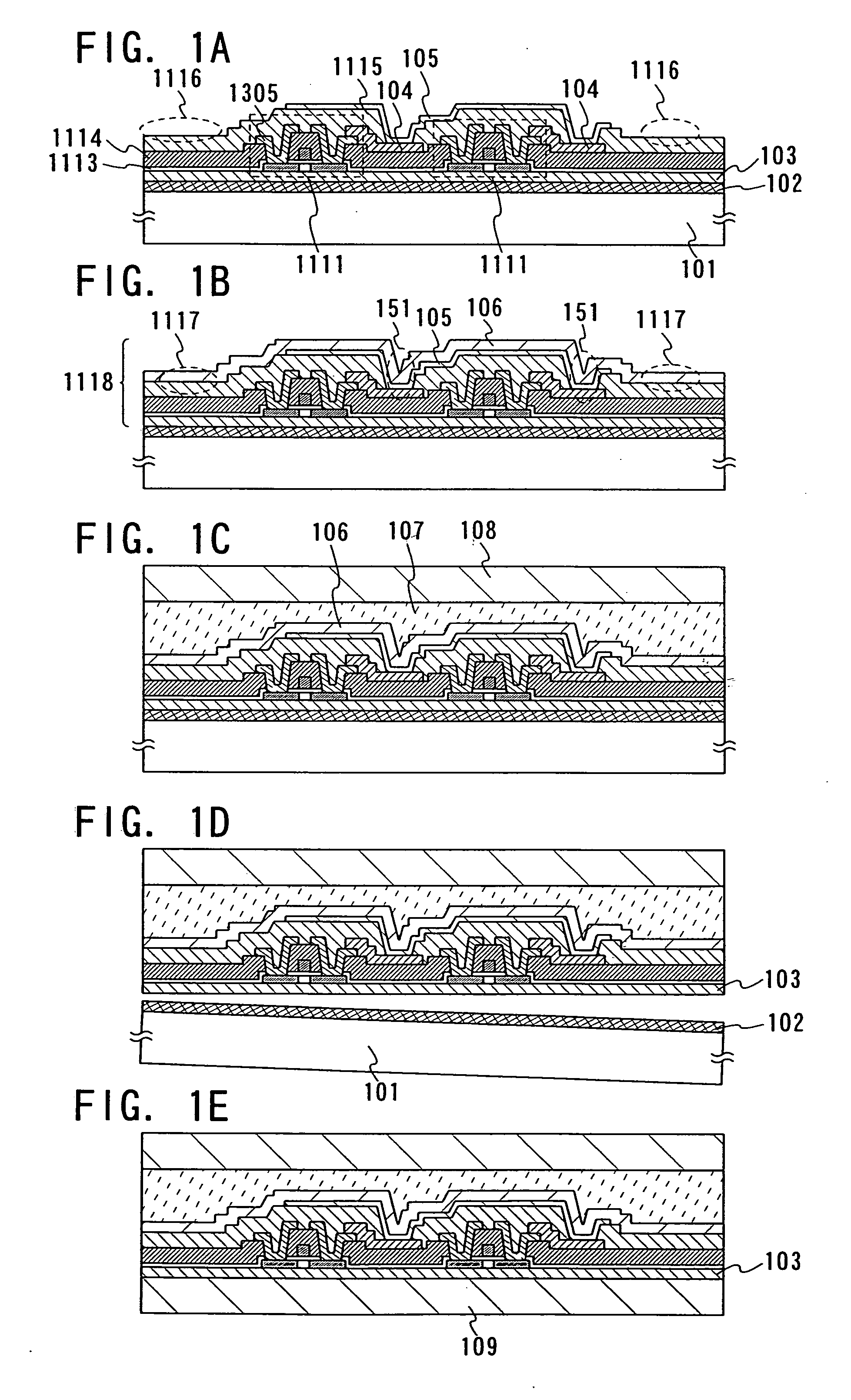
[0059] With reference to FIGS. 1A to 1E, this embodiment mode will describe a method for separating, with high yield, an element which has a layer containing an organic compound and an element-forming layer having the element.

[0060] As shown in FIG. 1A, a separation layer 102 is formed over a substrate 101, and an insulating layer 103 is formed over the separation layer 102. Next, a semiconductor element is formed over the insulating layer 103. Here, a thin film transistor 1111 is formed as the semiconductor element. Then, a first electrode layer 104 which is to be connected to a wire 1305 of the thin film transistor 1111 is formed, and an inorganic insulating layer 1115 covering an end portion of the first electrode layer 104 is formed. A layer 105 containing an organic compound is formed over the first electrode layer 104 and the inorganic insulating layer 1115 by an evaporation method. In FIG. 1A, a region 1116 is a region where the inorganic insulating layer 1115 is exposed. Th...

embodiment mode 2

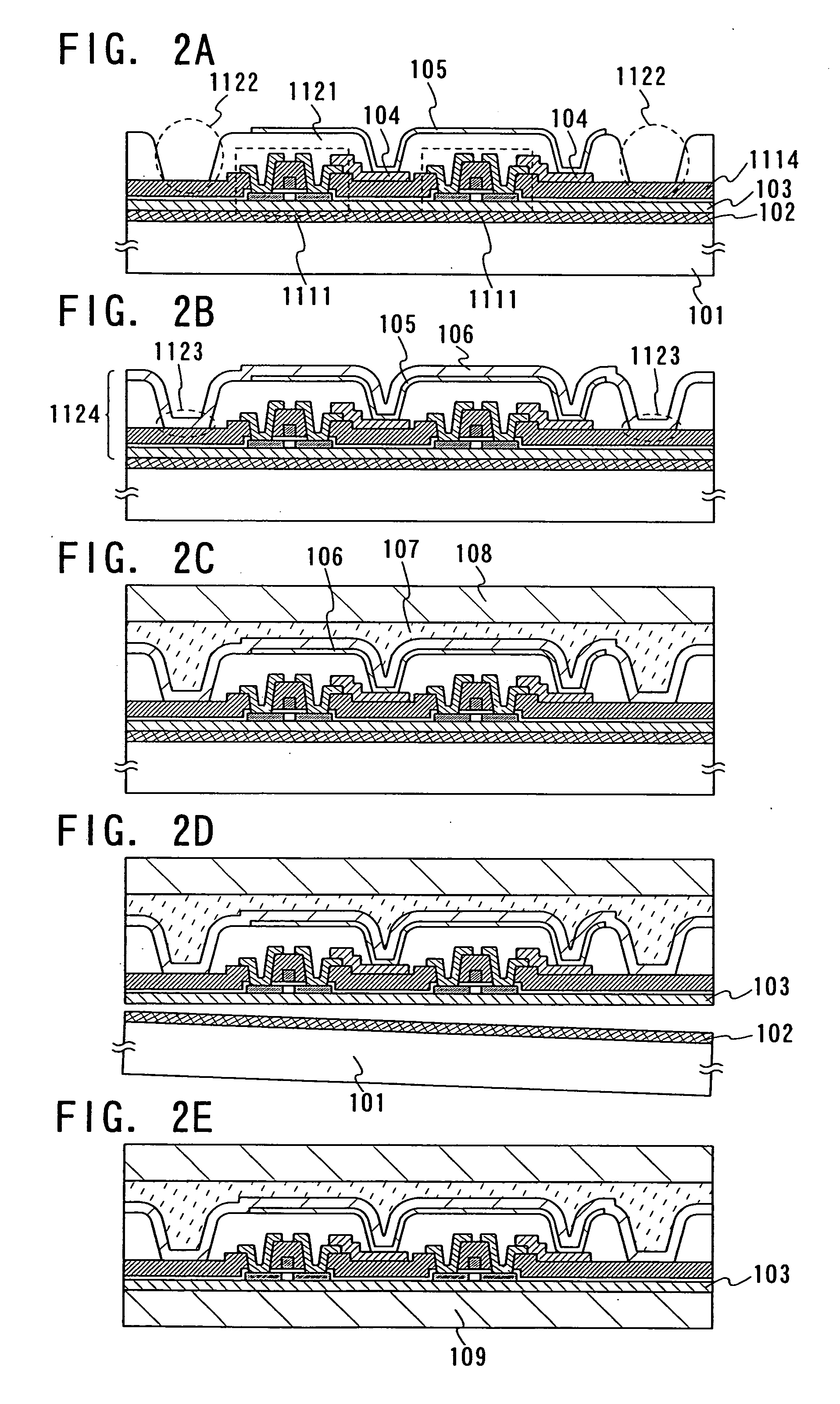
[0132] With reference to FIGS. 2A to 2E, this embodiment mode will describe a method for separating an element-forming layer, which is different from that in Embodiment Mode 1. This embodiment mode is different from Embodiment Mode 1 in that an organic insulating layer is formed instead of the inorganic insulating layer which covers an end portion of the first electrode layer.

[0133] As shown in FIG. 2A, the separation layer 102 is formed over the substrate 101, the insulating layer 103 is formed over the separation layer 102, and the thin film transistor 1111 is formed over the insulating layer 103, similarly to Embodiment Mode 1. In this embodiment mode, an interlayer insulating layer for insulating a gate electrode from a wire of the thin film transistor 1111 is formed by using an inorganic insulating layer 1114, similarly to Embodiment Mode 1. Next, the first electrode layer 104 is formed over the inorganic insulating layer 1114.

[0134] Subsequently, an organic insulating layer ...


PUM

PropertyMeasurementUnit
lengthaaaaaaaaaa
temperatureaaaaaaaaaa
work functionaaaaaaaaaa

Abstract

It is an object of the present invention to manufacture, with high yield, semiconductor devices in each of which an element which has a layer containing an organic compound is provided over a flexible substrate. A method for manufacturing a semiconductor device includes: forming a separation layer over a substrate; forming an element-forming layer by forming an inorganic compound layer, a first conductive layer, and a layer containing an organic compound over the separation layer, and forming a second conductive layer which is in contact with the layer containing an organic compound and the inorganic compound layer; and after attaching a first flexible substrate over the second conductive layer, separating the separation layer and the element-forming layer at the separation layer.

Description

BACKGROUND OF THE INVENTION [0001] 1. Field of Invention [0002] The present invention relates to a semiconductor device provided with an element which has a layer containing an organic compound over a flexible substrate, and also relates to a manufacturing method of the semiconductor device. [0003] 2. Description of the Related Art [0004] In recent years, development has been advanced on semiconductor devices which have various functions by integrating a plurality of circuits over insulating surfaces. Moreover, development has also been advanced on semiconductor devices which can send and receive data wirelessly by providing antennas. Such semiconductor devices are referred to as wireless chips (also referred to as ID tags, IC tags, IC chips, RF (Radio Frequency) tags, wireless tags, electronic tags, or RFID (Radio Frequency Identification) tags) and have been already introduced into some markets. [0005] Many of these semiconductor devices which have been put into practical use have...

Claims


Application Information

Patent Timeline
Patent Type & Authority Applications(United States)
IPC IPC(8): H01L29/08H05B44/00
CPCH01L27/12H01L27/1266H01L27/1292H01L27/1285H01L29/78603H01L27/1244
Inventor SUZUKI, TSUNENORINOMURA, RYOJIYUKAWA, MIKIOOHSAWA, NOBUHARUTAKANO, TAMAEASAMI, YOSHINOBUSATO, TAKEHISA
Owner SEMICON ENERGY LAB CO LTD
Why Eureka
Try Eureka