

FinFET and method for manufacturing the same
- Summary
- Abstract
- Description
- Claims
- Application Information
AI Technical Summary
Benefits of technology
Problems solved by technology
Method used
Image

Examples
first embodiment
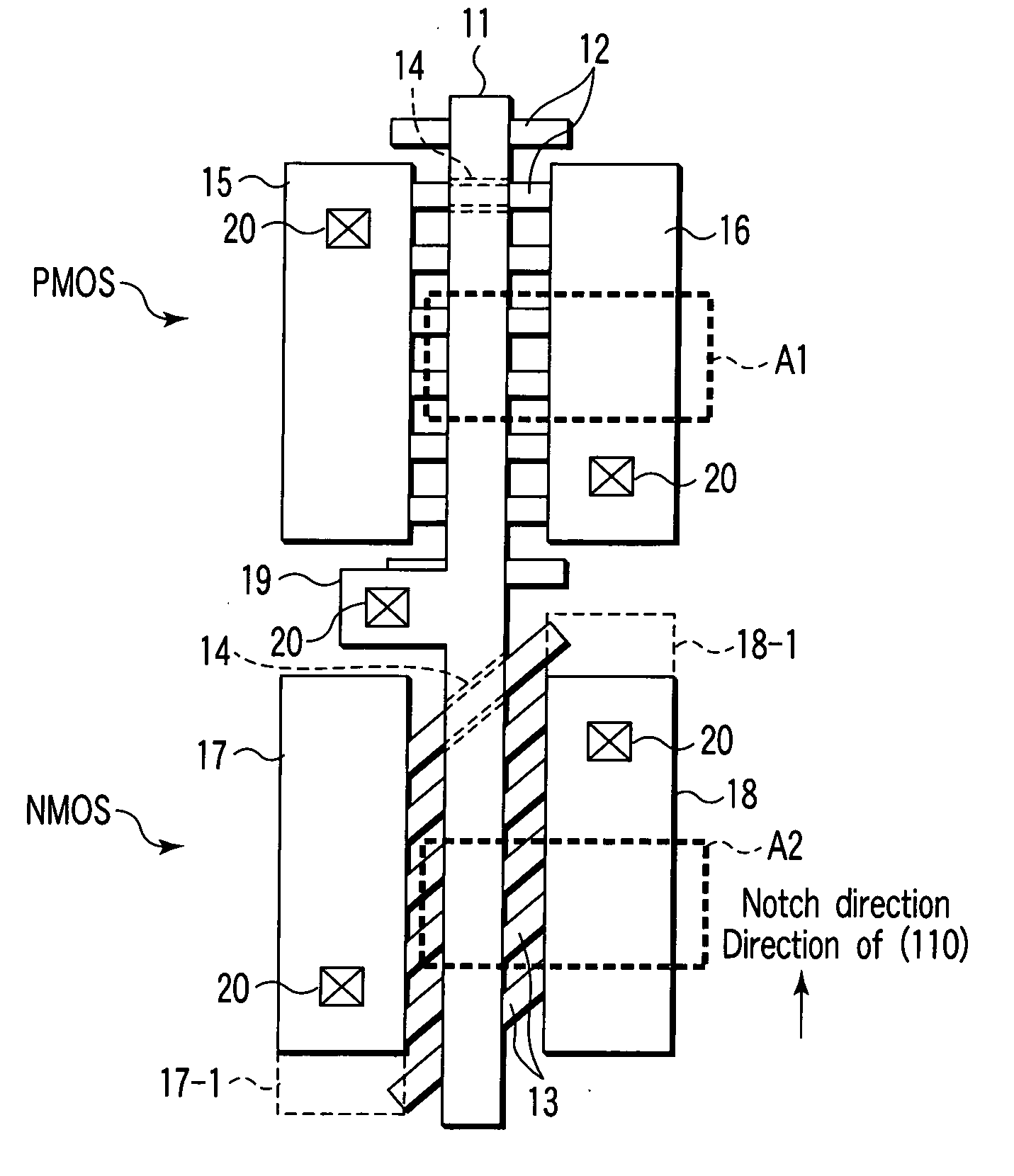
[0044]FIG. 1 shows a first embodiment, an example of a CMOS inverter using a FinFET.
[0045] Referring to FIG. 1, a gate electrode 11 is formed along a notch direction ((110) direction) on a substrate (not shown), which is a normal wafer having the surface orientation (100). A plurality of Fins 12, which are active regions of a PMOS-FinFET and serve as channel regions, are formed perpendicular to the gate electrode 11. Therefore, the side surfaces of the Fins 12 extend along a (110) plane. A plurality of Fins 13, which are active regions of an NMOS-FinFET and serve as channel regions, are inclined relative to the gate electrode 11. More specifically, the Fins 13 are inclined by about 45 degrees relative to the gate electrode 11. Therefore, the side surfaces of the Fins 13 extend along the (100) plane. The angle of the Fins 13 with respect to the gate electrode 11 may be 45±10 degrees, in which case a desired effect can be obtained.
[0046] A gate insulation film 14, indicated by broke...
second embodiment
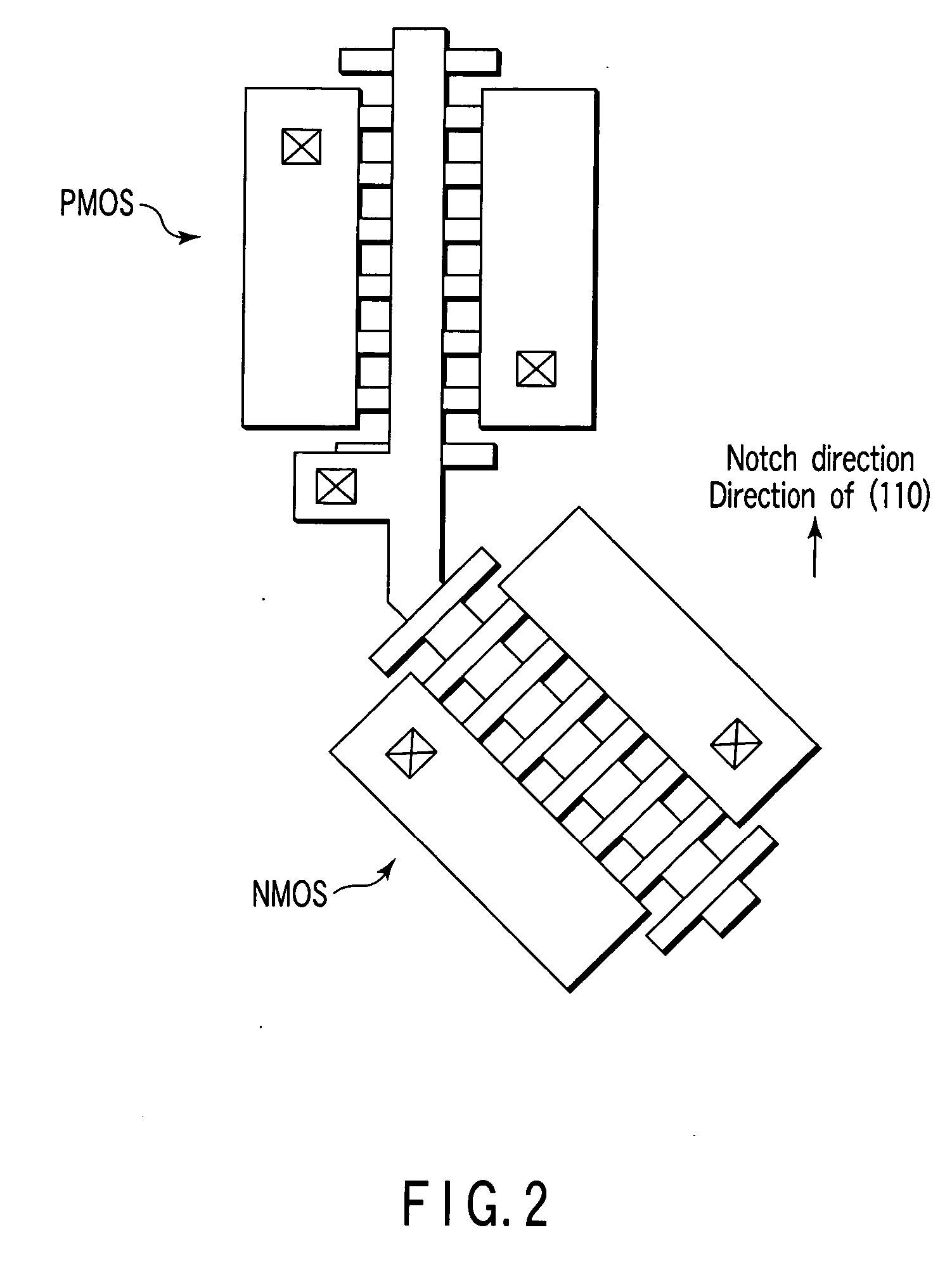
[0053]FIG. 3 shows a second embodiment. In the first embodiment, the Fins 13 of the NMOS are inclined relative to the gate electrode 11. In contrast, in the second embodiment, the Fins of the PMOS are inclined relative to the gate electrode 11. The portions of the second embodiment that are the same as those in the first embodiment are identified by the same reference numerals as those used for the first embodiment.
[0054] The second embodiment is different from the first embodiment in that the notch or orientation flat of the wafer is shifted by 45 degrees; that is, the notch direction is the direction of (100). As shown in FIG. 3, the gate electrode 11 extends in the notch direction (the direction of (100)). Therefore, the side surfaces of the Fins 12 extend along the (110) plane. The Fins 13 of the NMOS-FinFET are perpendicular to the gate electrode 11. Therefore, the side surfaces of the Fins 13 extend along the (100). The angle of the Fins 12 with respect to the gate electrode ...
third embodiment
[0057]FIGS. 4A and 4B show a third embodiment of the present invention, in which, for example, the structure of the first embodiment is applied to a NAND gate and a NOR gate. FIG. 4A shows an example of a NAND circuit using two CMOS inverter circuits, and FIG. 4B shows an example of a NOR circuit using two CMOS inverter circuits. In FIGS. 4A and 4B, the portions that are the same as those in the first embodiment are identified by the same reference numerals as those used for the first embodiment.
[0058] Referring to FIGS. 4A and 4B, gate electrodes 11-1 and 11-2 are arranged along, for example, the notch direction (the direction of (110)). The Fins 12 of the PMOS-FinFET are perpendicular to the gate electrodes 11-1 and 11-2, while the Fins 13 of the NMOS-FinFET are inclined relative to the gate electrodes 11-1 and 11-2. More specifically, the Fins 13 are inclined by, for example, 45 degrees (±10 degrees) relative to the gate electrodes 11-1 and 11-2.
[0059] The NAND circuit and the ...
PUM
 Abstract
Description
Claims
Application Information