Complementary field-effect transistors and methods of manufacture

a technology of complementary field effect transistors and manufacturing methods, applied in the direction of transistors, semiconductor devices, electrical apparatus, etc., can solve the problems of high defect density of substrates, limited approach, cost and fundamental material properties, etc., to improve the operating characteristics of semiconductor devices and a method.

Inactive Publication Date: 2005-06-02
TAIWAN SEMICON MFG CO LTD
View PDF11 Cites 80 Cited by
  • Summary
  • Abstract
  • Description
  • Claims
  • Application Information

AI Technical Summary

Benefits of technology

[0008] These and other problems are generally reduced, solved or circumvented, and technical advantages are generally achieved, by embodiments of the present invention, which provides a strained semiconductor device to improve the operating characteristics of the semiconductor device and a method of manufacture.

Problems solved by technology

This approach is very expensive because a SiGe buffer layer with thickness in the order of micrometers has to be grown.
Numerous dislocations in the relaxed SiGe buffer layer exist and some of these dislocations propagate to the strained silicon layer, resulting in a substrate with high-defect density.
Thus, this approach has limitations that are related to cost and fundamental material properties.
The high stress film or stressor exerts significant influence on the channel, modifying the silicon lattice spacing in the channel region, and thus introducing strain in the channel region.
However, uniaxial tensile strain degrades the hole mobility while uniaxial compressive strain degrades the electron mobility.
Ion implantation of germanium can be used to selectively relax the strain so that the hole or electron mobility is not degraded, but this is difficult to implement due to the close proximity of the n-channel and p-channel transistors.

Method used


Image

  • Complementary field-effect transistors and methods of manufacture
  • Complementary field-effect transistors and methods of manufacture
  • Complementary field-effect transistors and methods of manufacture

Examples


Embodiment Construction

[0017] The making and using of the presently preferred embodiments are discussed in detail below. It should be appreciated, however, that the present invention provides many applicable inventive concepts that can be embodied in a wide variety of specific contexts. The specific embodiments discussed are merely illustrative of specific ways to make and use the invention, and do not limit the scope of the invention.

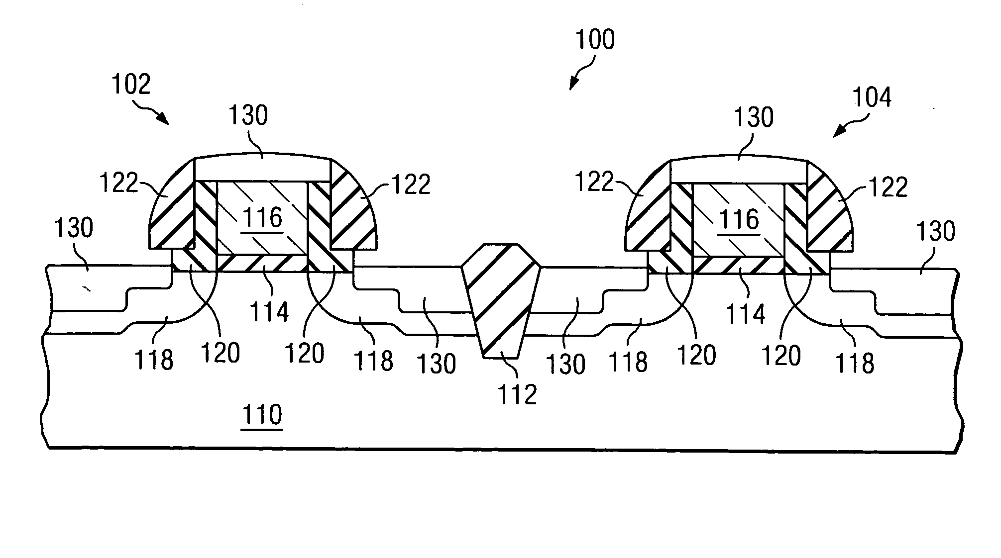
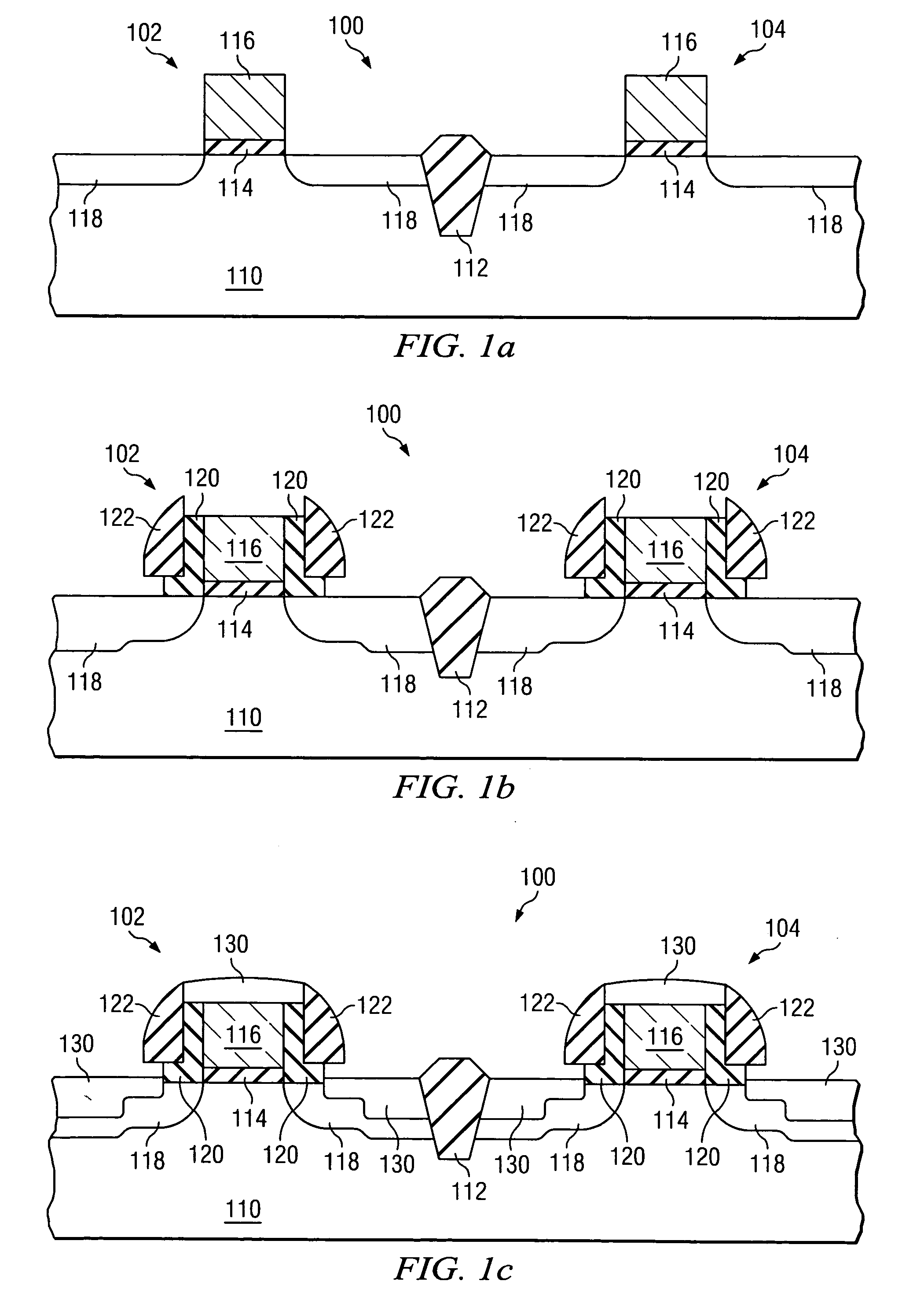
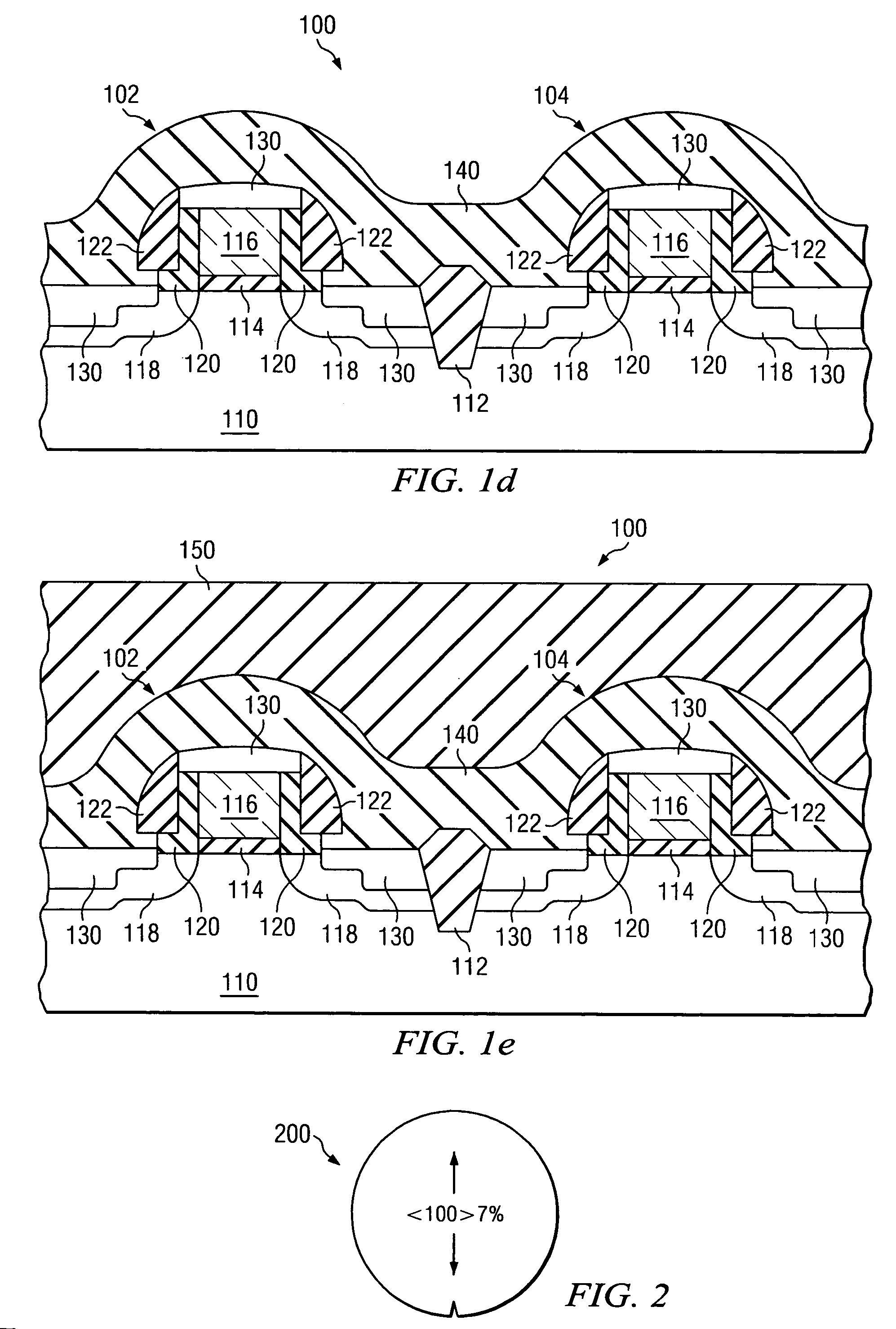
[0018]FIGS. 1a-1e illustrate a first method embodiment for fabricating strained channel regions of transistors in a semiconductor chip. Embodiments of the present invention illustrated herein may be used in a variety of circuits. For example, embodiments of the present invention may be utilized to form circuits for NOR gates, logic gates, inverters, XOR gates, NAND gates, PMOS transistors for pull-up transistor, NMOS transistor for pull-down transistor, and the like.

[0019] Referring first to FIG. 1a, a wafer 100 is shown comprising a first transistor 102 and a second trans...


PUM

PropertyMeasurementUnit
tensile stressaaaaaaaaaa
surface roughnessaaaaaaaaaa
dielectric constantaaaaaaaaaa

Abstract

A complementary FET and a method of manufacture is provided. The complementary FET utilizes a substrate having a surface layer with a <100> crystal orientation. Tensile stress, which increases performance of the NMOS FETs, is added by silicided source/drain regions, tensile-stress film, shallow trench isolations, inter-layer dielectric, or the like.

Description

[0001] This application claims the benefit of U.S. Provisional Application No. 60 / 526,133 filed on Dec. 1, 2003, entitled Complementary Field-Effect Transistors and Method of Manufacture, which application is hereby incorporated herein by reference.TECHNICAL FIELD [0002] The present invention relates generally to semiconductor devices, and more particularly, to complementary field-effect transistors and methods of manufacture. BACKGROUND [0003] Size reduction of metal-oxide-semiconductor field-effect transistors (MOSFET), including reduction of the gate length and gate oxide thickness, has enabled the continued improvement in speed, performance, density, and cost per unit function of integrated circuits over the past few decades. To further enhance transistor performance, strain may be introduced in the transistor channel for improving carrier mobilities. Generally, it is desirable to induce a tensile strain in the n-channel of an NMOS transistor in the source-to-drain direction, an...

Claims


Application Information

Patent Timeline
Patent Type & Authority Applications(United States)
IPC IPC(8): H01L21/336H01L21/76H01L21/8238H01L27/092H01L29/78H01L31/0328
CPCH01L21/823807H01L21/823814H01L21/823864H01L29/045H01L29/7845H01L29/6656H01L29/6659H01L29/7833H01L29/7843H01L29/665
Inventor HUANG, CHIEN-CHAOYANG, FU-LIANGKEN, MICKEYHU, CHENMINGGE, CHUNG-HULEE, WEN-CHINKO, CHIH-HSIN
Owner TAIWAN SEMICON MFG CO LTD
Why Eureka
Try Eureka