Method of manufacturing epitaxial silicon wafer and apparatus thereof

a manufacturing method and silicon wafer technology, applied in the direction of crystal growth process, polycrystalline material growth, chemically reactive gas, etc., can solve the problems of difficult to say that the thickness is good enough, difficult to secure the flatness of the edge part, and difficult to achieve the thickness uniformity of the layer, etc., to achieve the effect of improving the thickness of the epitaxial silicon wafer

Active Publication Date: 2007-10-04
SUMCO TECHXIV
View PDF5 Cites 76 Cited by
  • Summary
  • Abstract
  • Description
  • Claims
  • Application Information

AI Technical Summary

Benefits of technology

[0011] In consideration of the aforementioned, an apparatus and a method for forming an epitaxial layer to improve uniformization of the thickness of an epitaxial silicon wafer and, in particular, an apparatus and a method for controlling the epitaxial layer thickness of a wafer edge part may be provided.

Problems solved by technology

However, it is likely that the edge part of a silicon single crystal wafer to serve as a substrate shows an abrupt change in the thickness of the formed epitaxial layer and hence it is difficult to secure the flatness in the edge part.
Moreover, since it is likely that the vicinity of the edge part (or the outer circumferential part) of a semiconductor wafer (for example, a silicon single crystal wafer) to serve as a substrate shows an abrupt change in the thickness of the formed epitaxial layer due to various factors, and it is difficult to achieve the layer thickness uniformity only by the uniformization of the flow of gas for epitaxial growth.
Therefore, a number of methods of optimizing epitaxial growth conditions to reduce the unevenness in the distribution of the layer thickness have been proposed, but it is hard to say that they are good enough.
Since a flattening process after the epitaxial growth cannot be performed when the grown wafer is found to have unsatisfactory flatness is obtained.
Therefore, such wafer is deemed to be defective so as to become a waste.
However, Japanese Unexamined Patent Application Publication No. 2001-302395 does not disclose concretely a method of simulating film formation in the epitaxial growth.
In general, simulation of the layer formation is not necessarily easy since various factors interact with each other.
Therefore, it is very difficult, by using the method of Japanese Unexamined Patent Application Publication No. 2005-353665, to perform the simulation in order to predict the flatness of the epitaxial silicon wafer on which the epitaxial layer is formed.

Method used


Image

  • Method of manufacturing epitaxial silicon wafer and apparatus thereof
  • Method of manufacturing epitaxial silicon wafer and apparatus thereof
  • Method of manufacturing epitaxial silicon wafer and apparatus thereof

Examples


example 1

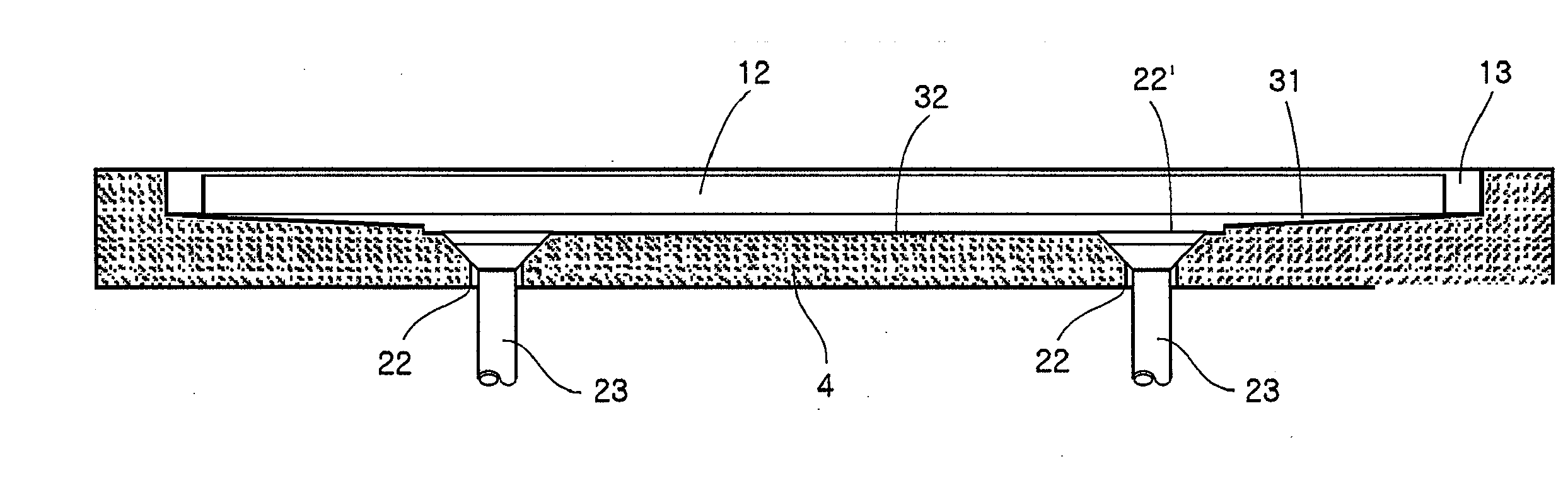
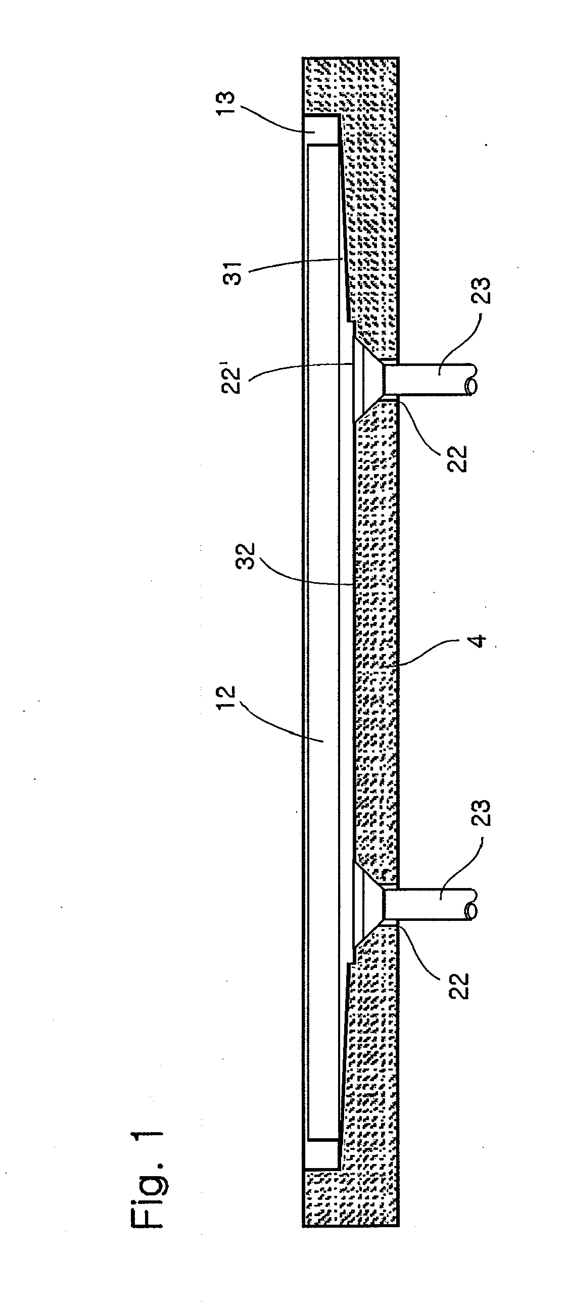
[0104] FIGS. 13 to 17 show layer thickness distribution when an epitaxial layer is formed by changing spot facing depth. Duplicated explanation thereof is omitted because of similarity to FIGS. 5 and 6. FIGS. 13 and 14 show a partial enlarged cross section of a susceptor and the like, and FIG. 15 is a top view of the susceptor 4. FIG. 16 is a graph showing spot facing depth and being developed with respect to the angle. The spot facing depth of the present case is made smaller at shallow parts than the thickness D1 of a semiconductor wafer 12. As shown in FIGS. 15 and 16, the spot facing depth changes with a cycle of about 90 degrees.

[0105] In a (100) substrate (notch direction 0°) which is the semiconductor wafer, the growth rate of the epitaxial layer of an edge part becomes gradually slower as the direction changes from 0° to 45°. The susceptor was machined so as to minimize the spot facing depth of the portion in which the direction of 45° of the wafer is located when the wafer...

example 2

[0106] FIGS. 18 to 20A and 21A show layer thickness distribution when an epitaxial layer is formed by changing pocket width. Duplicated explanation is omitted because of similarity to FIGS. 7 and 8. FIGS. 18 and 19 show a partial enlarged cross section view of a susceptor and the like, and FIG. 20 is a top view of the susceptor 4. FIG. 21A is a graph showing the effect of pocket width on layer thickness and being developed with respect to the angle. The pocket width in this experiment is made slightly wider than the radius of a semiconductor wafer 12 at a narrow part, and about 5 mm wider than the above diameter at a wide part. As shown in FIG. 20A, the pocket width changes with a cycle of 90 degrees.

[0107] In a (100) substrate (notch direction 0°) which is a semiconductor wafer, the growth rate of the epitaxial layer of an edge part becomes gradually smaller as the direction changes from 0° to 45°. The susceptor was machined so as to maximize the pocket width of the portion in whi...

example 3

[0113] FIGS. 22 to 26 show layer thickness distribution as an epitaxial layer is formed by changing thermal capacity (partial thickness of susceptor). Duplicated explanation thereof is omitted because of the similarity to FIGS. 9 and 10. FIGS. 22 and 23 show a partial enlarged cross section view of a susceptor and the like, and FIG. 24 is a schematic diagram of the bottom of the susceptor 4. FIG. 25 shows the variation of susceptor thickness developed with respect to the angle. FIG. 26 is a graph showing the effect of susceptor thickness on layer thickness developed with respect to the angle. In this susceptor, the partial thickness of a thick portion is about 20% larger than the partial thickness of a thin portion. As FIGS. 24 and 25 show, the thickness of the susceptor changes with a cycle of about 90 degrees.

[0114] In a (100) substrate (notch direction 0°) which is a semiconductor wafer, the growth rate of the epitaxial layer of an edge part becomes gradually smaller as the dire...


PUM

PropertyMeasurementUnit
temperatureaaaaaaaaaa
lengthaaaaaaaaaa
lengthaaaaaaaaaa

Abstract

A method of forming an epitaxial layer to increase flatness of an epitaxial silicon wafer is provided. In particular, a method of controlling the epitaxial layer thickness in a peripheral part of the wafer is provided. An apparatus for manufacturing an epitaxial wafer by growing an epitaxial layer with reaction of a semiconductor wafer and a source gas in a reaction furnace comprising: a pocket in which the semiconductor wafer is placed; a susceptor fixing the semiconductor; orientation-dependent control means dependent on a crystal orientation of the semiconductor wafer and/or orientation-independent control means independent from the crystal orientation of the semiconductor wafer, wherein the apparatus may improve flatness in a peripheral part of the epitaxial layer.

Description

CROSS REFERENCE TO RELATED APPLICATIONS [0001] This application is based upon and claims the benefits of priorities from Japanese Patent Application Nos. 2006-95717 and 2006-95718 filed on Mar. 30, 2006, the entire contents of which are incorporated herein by reference. FIELD OF THE INVENTION [0002] The present invention relates to a method and apparatus for manufacturing an epitaxial wafer, and more specifically relates to the method and apparatus for manufacturing an epitaxial wafer with high flatness. RELATED ART [0003] In general, the epitaxial silicon wafer has excellent characteristics such that neither defects arising from oxygen nor Grown-in defects (including COP) introduced during single crystal ingot growth are included in a surface epitaxial layer thereof where the device is made. [0004] In recent years, epitaxial silicon wafers are being used for high-performance devices such as MPUs and flash memories and high-performance power devices such as MOS FETs and IGBTs. On th...

Claims


Application Information

Patent Timeline
Patent Type & Authority Applications(United States)
IPC IPC(8): C30B23/00C30B25/00C30B28/12C23C16/00
CPCC23C16/24C23C16/4585C30B25/12C30B23/063C23C16/4586H01L21/68735
Inventor NARAHARA, KAZUHIROKATO, HIROTAKAHAYASHIDA, KOICHIRO
Owner SUMCO TECHXIV
Why Eureka
Try Eureka