Dual SIMOX hybrid orientation technology (HOT) substrates

a technology of hybrid orientation and substrate, applied in the direction of semiconductor devices, basic electric elements, electrical appliances, etc., can solve the problems of significant deformation of electron mobilities on (110) si surfaces, undesirable width of pfets, and inability to adapt to nfet devices, etc., to achieve the effect of improving the performance of each devi

Inactive Publication Date: 2006-02-02
IBM CORP
View PDF3 Cites 74 Cited by
  • Summary
  • Abstract
  • Description
  • Claims
  • Application Information

AI Technical Summary

Benefits of technology

[0021] One object of the present invention is to provide a method of fabricating integrated semiconductor devices such that different types of CMOS devices are formed upon a specific crystal orientation of a silicon-on-insulator (SOI) substrate that enhances the performance of each device.

Problems solved by technology

To compensate for this discrepancy, pFETs are typically designed with larger widths in order to balance pull-up currents against the nFET pull-down currents and achieve uniform circuit switching. pFETs having larger widths are undesirable since they take up a significant amount of chip area.
Unfortunately, electron mobilities on (110) Si surfaces are significantly degraded compared to (100) Si surfaces.
As can be deduced from the above, the (110) Si surface is optimal for pFET devices because of excellent hole mobility, yet such a crystal orientation is completely inappropriate for NFET devices.
A drawback of the method described above and illustrated in FIGS. 1A-1F is that the processing leaves only one of the semiconductor orientations disposed on a BOX. FIGS. 2A-2F show the additional masking and SIMOX (separation by implanted oxygen) steps described in U.S. application Ser. No. 10 / 634,446 that can be applied to the structure of FIG.
A drawback of the approach described above and illustrated in FIGS. 2A-2E is that it requires additional masking layers to protect the semiconductor layer 40 from the SIMOX implant and anneal.

Method used


Image

  • Dual SIMOX hybrid orientation technology (HOT) substrates
  • Dual SIMOX hybrid orientation technology (HOT) substrates
  • Dual SIMOX hybrid orientation technology (HOT) substrates

Examples


Embodiment Construction

[0045] The present invention, which provides double SIMOX HOT (hybrid orientation technology) substrates, will now be described in more detail by referring to the drawings that accompany the present application. In the accompanying drawings, like and corresponding elements are referred to by like reference numerals. It is noted that the drawings of the present application are provided for illustrative purposes and are thus not drawn to scale.

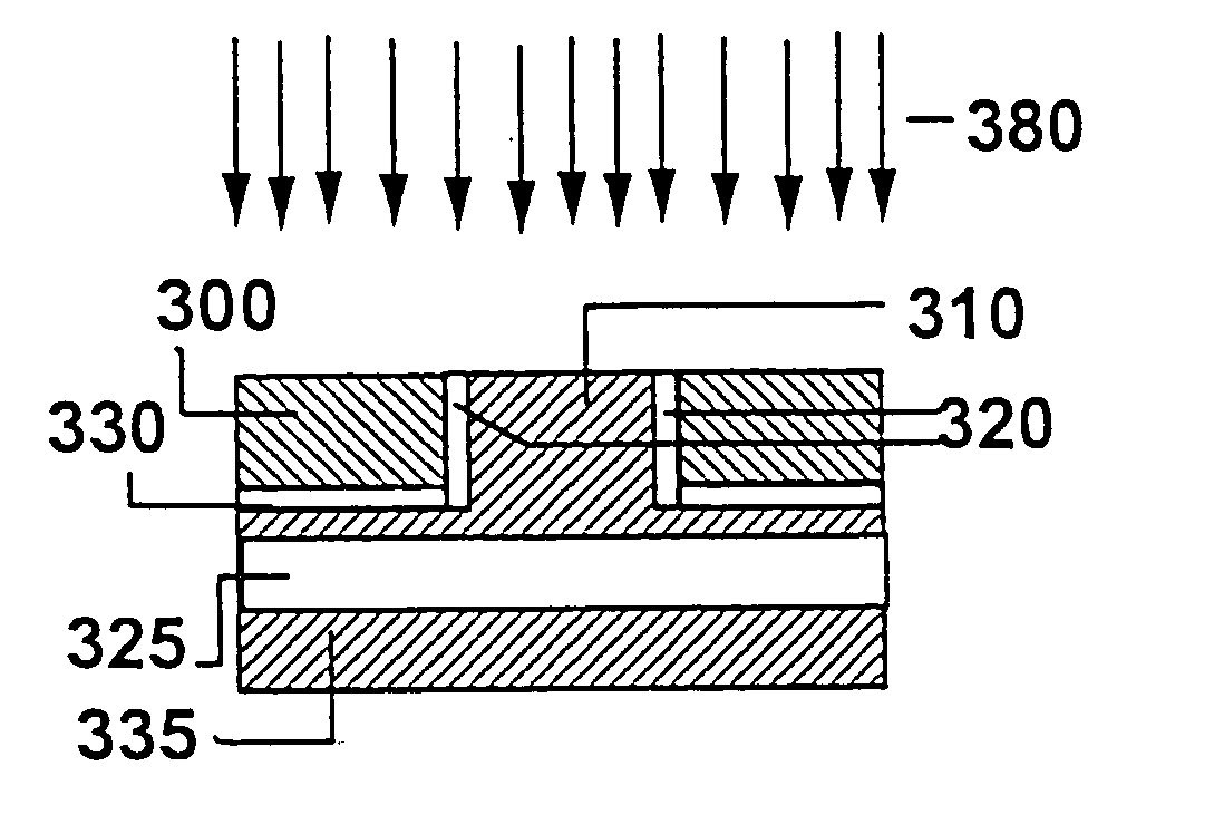
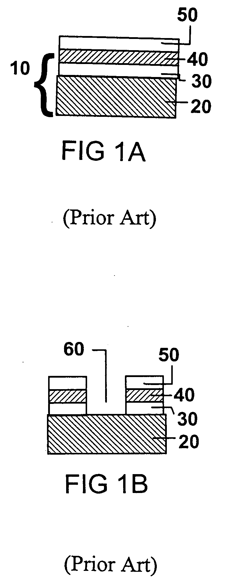
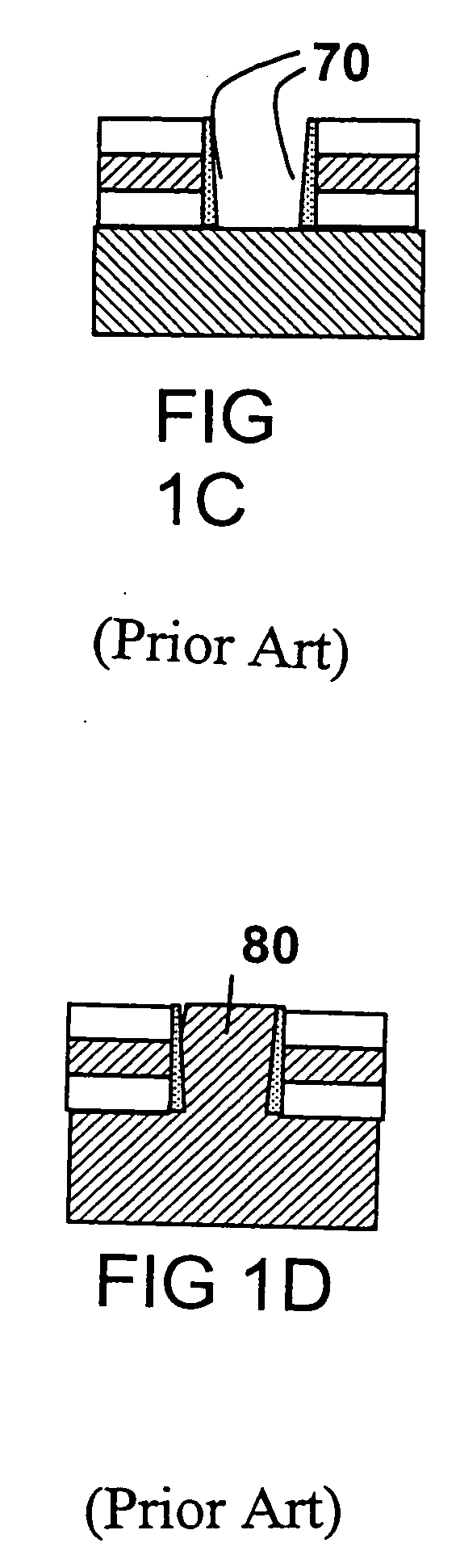
[0046]FIGS. 4A-4H show, in cross section view, possible initial substrates that can be employed in the present invention. The initial substrates of FIGS. 4A-4H are all planar, hybrid orientation substrates comprising a base semiconductor substrate layer 20 having a first orientation, and one or more top semiconductor layers or regions 300 having a second orientation different from the first orientation. The one or more top semiconductor regions 300 are typically formed by bonding utilizing the procedures described in the '241 application that w...


PUM


Abstract

This invention provides a separation by implanted oxygen (SIMOX) method for forming planar hybrid orientation semiconductor-on-insulator (SOI) substrates having different crystal orientations, thereby making it possible for devices to be fabricated on crystal orientations providing optimal performance. The method includes the steps of selecting a substrate having a base semiconductor layer having a first crystallographic orientation separated by a thin insulating layer from a top semiconductor layer having a second crystallographic orientation; replacing the top semiconductor layer in selected regions with an epitaxially grown semiconductor having the first crystallographic orientation; then using an ion implantation and annealing method to (i) form a buried insulating region within the epitaxially grown semiconductor material, and (ii) thicken the insulating layer underlying the top semiconductor layer, thereby forming a hybrid orientation substrate in which the two semiconductor materials with different crystallographic orientations have substantially the same thickness and are both disposed on a common buried insulator layer. In a variation of this method, an ion implantation and annealing method is instead used to extend an auxiliary buried insulator layer (initially underlying the base semiconductor layer) upwards (i) into the epitaxially grown semiconductor, and (ii) up to the insulating layer underlying the top semiconductor layer.

Description

RELATED APPLICATIONS [0001] This application is related to co-pending and co-assigned U.S. patent application Ser. No. 10 / 250,241, filed Jun. 17, 2003 entitled “High-performance CMOS SOI devices on hybrid crystal-oriented substrates,” co-pending and co-assigned U.S. patent application Ser. No. 10 / 634,446, filed Aug. 5, 2003 entitled “Self-aligned SOI with different crystal orientation using wafer bonding and SIMOX processes,” and co-pending and co-assigned U.S. patent application Ser. No. 10 / 725,850, filed Dec. 2, 2003 entitled “Planar substrate with selected semiconductor crystal orientations formed by localized amorphization and recrystallization of stacked template layers.” The entire content of each of the three applications mentioned above is incorporated by reference. [0002] The '241 application describes an epitaxial growth method for making a planar hybrid orientation substrate which comprises one or more regions of a first single-crystal semiconductor disposed on bulk silic...

Claims


Application Information

Patent Timeline
Patent Type & Authority Applications(United States)
IPC IPC(8): H01L21/20H01L21/425H01L21/762H01L21/84
CPCH01L21/76243H01L21/76267H01L27/1207H01L27/1203H01L21/84
Inventor CHAN, KEVIN K.DE SOUZA, JOEL P.REZNICEK, ALEXANDERSADANA, DEVENDRA K.SAENGER, KATHERINE L.
Owner IBM CORP
Why Eureka
Try Eureka