

Device for electrostatic discharge protection
- Summary
- Abstract
- Description
- Claims
- Application Information
AI Technical Summary
Benefits of technology
Problems solved by technology
Method used
Image

Examples
Embodiment Construction
[0018] It is to be understood and appreciated that the circuit described below do not cover a complete circuit layout. The present invention can be practiced in conjunction with various circuit techniques that are used in the art, and only so much of the commonly practiced techniques are included herein to provide an understanding of the present invention.
[0019] The present invention will be described in detail with reference to the accompanying drawings. It should be noted that the drawings are in greatly simplified form and they are not drawn to scale. Moreover, dimensions have been exaggerated in order to provide a clear illustration and understanding of the present invention.
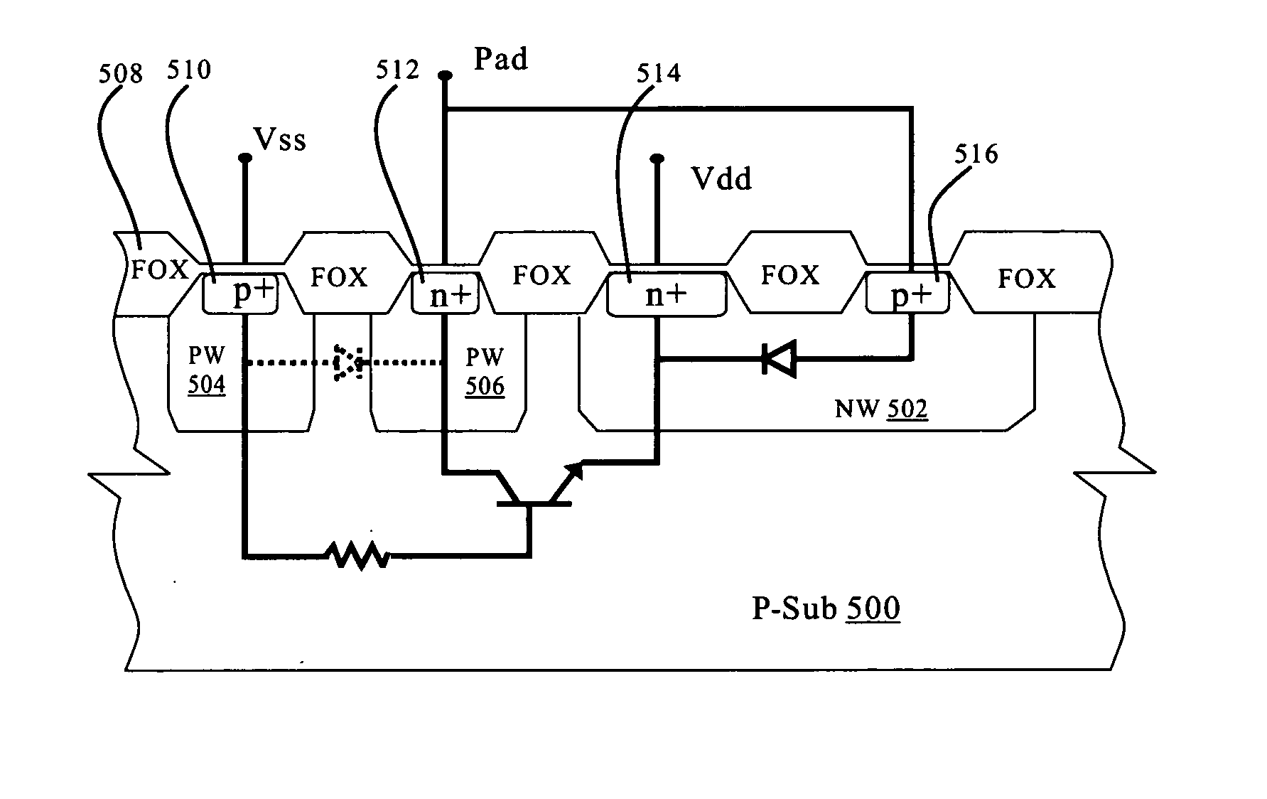
[0020] In one embodiment of the invention, the device for electrostatic discharge for protection of the invention further includes an N+ diffusion ring into a P well, wherein the N+ diffusion ring connects to a bond pad between the cathode of a diode and a P+ guard ring to for a parasitic lateral npn bipol...
PUM
 Abstract
Description
Claims
Application Information